 21
21
Gigabyte GeForce RTX 4060 WindForce OC Review
Test Setup »High-resolution PCB Pictures
These pictures are for the convenience of volt modders and people who would like to see all the finer details on the PCB. Feel free to link back to us and use these in your articles, videos or forum posts.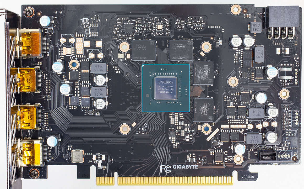

High-resolution versions are also available (front, back).
Circuit Board (PCB) Analysis
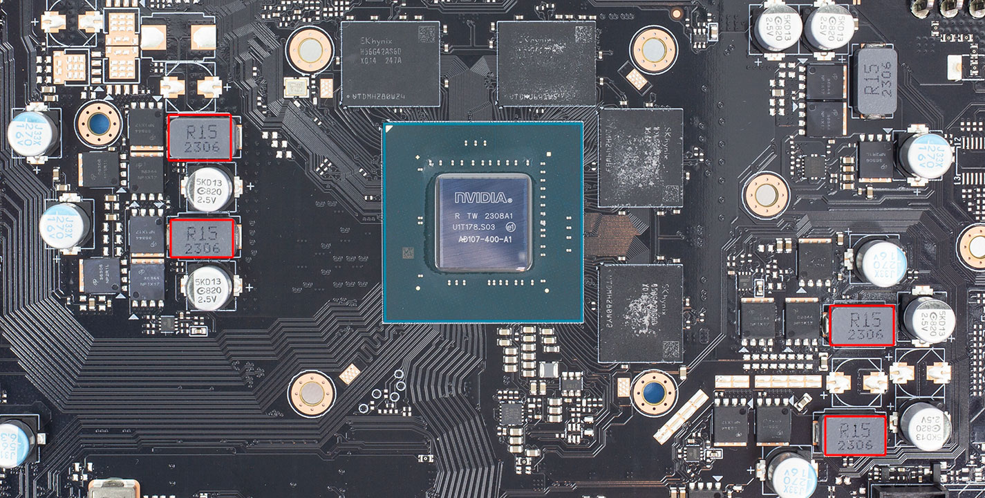

GPU voltage is handled by a 4-phase VRM driven by a UPI uP9512U controller.

A set of Alpha & Omega Semiconductor AONS36344/AONS36306 MOSFETs are used for the GPU power phases, these are each capable of 63 A.


Memory voltage is a single-phase design, and handled by a 7212 buck controller.

For memory, Gigabyte is using a set of Alpha & Omega Semiconductor AONS36344/AONS36306 MOSFETs, too, rated for 63 A.

The GDDR6 memory chips are made by Hynix and carry the model number H56G42AS6DX-014. They are specified to run at 2250 MHz (18 Gbps effective).

NVIDIA's AD107 graphics processor is the company's smallest Ada Lovelace GPU. It is built using a 5 nanometer process at TSMC Taiwan, with a transistor count of 18.9 million and a die size of 156 mm².
Jan 23rd, 2025 02:08 EST
change timezone
Latest GPU Drivers
New Forum Posts
- RDNA4 (RX 9070XT / 9070) launch announced for (delayed to) March 2025 (318)
- RDNA4 Prediction Time!!! (117)
- Last game you purchased? (630)
- Mobo choice for 12600k after returning MSI Tomahawk ( Broken M2 shield standoff ) (15)
- Stutters with New GPU (60)
- Post the idle temperature of your CPU (130)
- Free Games Thread (4396)
- Concerning noises on multiple motherboards, same CPU (7800X3D) (13)
- Mouse Suggestions and Recommendations ? (0)
- [Intel AX1xx/AX2xx/AX4xx/AX16xx/BE2xx/BE17xx] Intel Modded Wi-Fi Driver with Intel® Killer™ Features (252)
Popular Reviews
- NVIDIA GeForce RTX 5090 Founders Edition Unboxing
- NZXT C1500 Review
- Montech Heritage Pro Review - The Leather Case
- Alphacool Apex 1 CPU Water Block Review - Performance King!
- Pwnage StormBreaker Max CF Review
- PowerColor Alphyn AH10 Review
- AMD Ryzen 7 9800X3D Review - The Best Gaming Processor
- NVIDIA GeForce RTX 50 Technical Deep Dive
- ASRock Arc B570 Challenger OC Review
- Fosi Audio K7 Gaming Desktop DAC/Headphone Amplifier Review
Controversial News Posts
- NVIDIA 2025 International CES Keynote: Liveblog (470)
- AMD Debuts Radeon RX 9070 XT and RX 9070 Powered by RDNA 4, and FSR 4 (349)
- AMD Radeon RX 9070 XT & RX 9070 Custom Models In Stock at European Stores (226)
- NVIDIA GeForce RTX 5090 Features 575 W TDP, RTX 5080 Carries 360 W TDP (217)
- AMD Radeon RX 9070 XT Alleged Benchmark Leaks, Underwhelming Performance (204)
- AMD's Radeon RX 9070 Launch Faces Pricing Hurdles (174)
- Potential RTX 5090 and RTX 5080 Pricing in China Leaks (173)
- AMD Radeon RX 9070 XT Tested in Cyberpunk 2077 and Black Myth: Wukong (169)