 70
70
Gigabyte GeForce RTX 5090 Gaming OC Review
(70 Comments) »Introduction
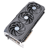
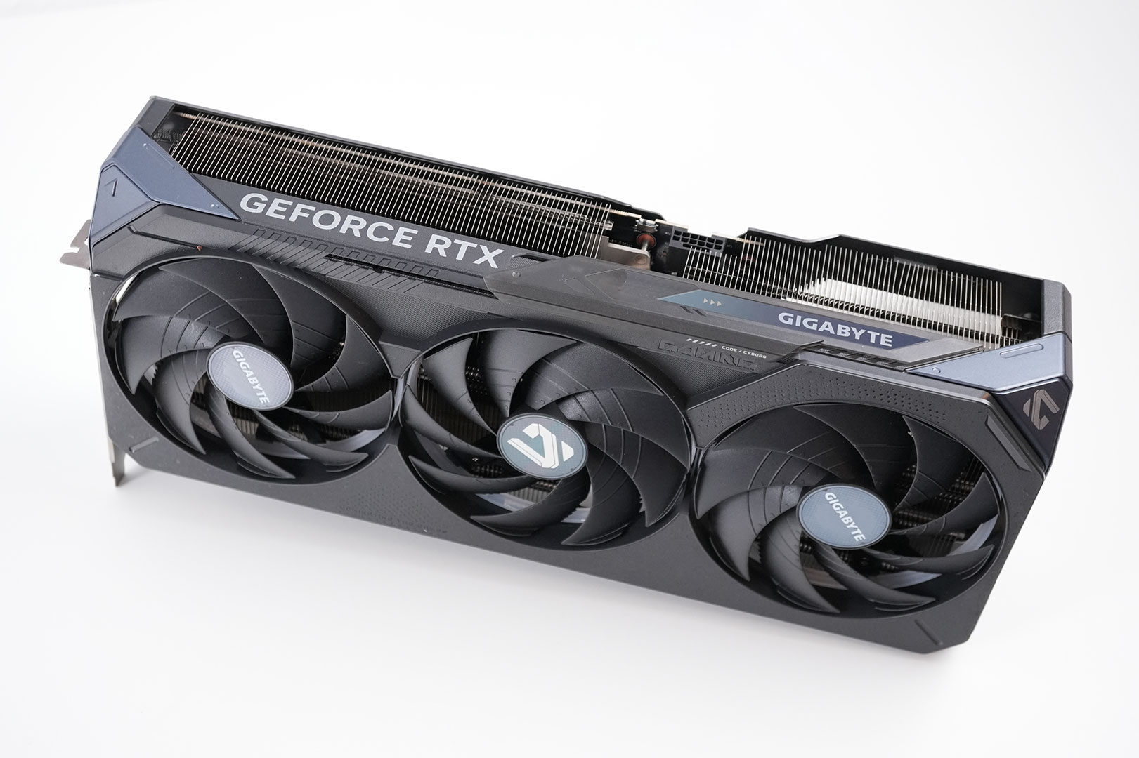
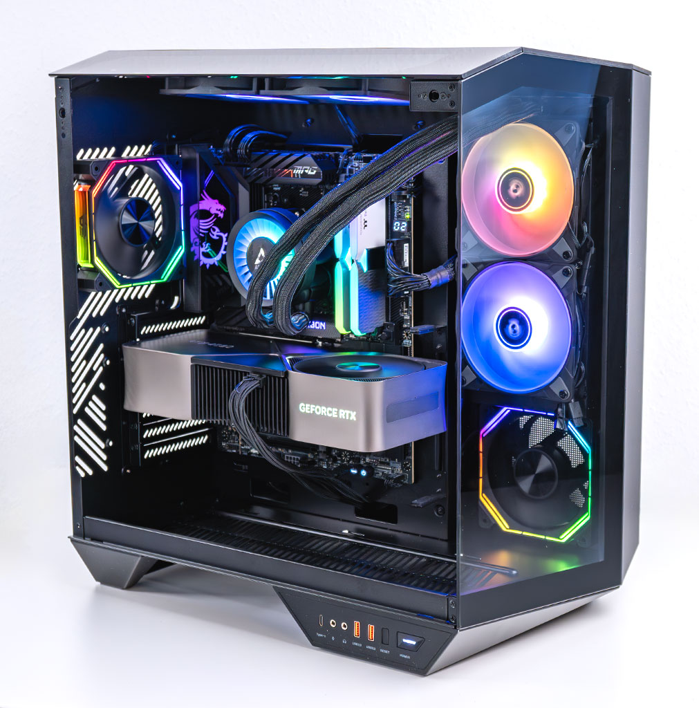
We have with us the Gigabyte GeForce RTX 5090 Gaming OC, the company's most affordable custom design take on this generation's flagship gaming GPU. The Gaming OC line of graphics cards by Gigabyte is positioned a notch below the company's AORUS Gaming series, targeting the class of buyers who have their minds set on a particular GPU, and don't need something swanky. These cards tend to be priced closest to the NVIDIA MSRP, which in case of the RTX 5090, is an eye-watering $2,000. The Gigabyte RTX 5090 Gaming OC is hardly a cheap product in that sense, and even within its price-point, it packs some serious kit, including a massive 4-slot cooling solution that uses a vapor chamber plate, multiple stacked heat pipes, a large aluminium fin-stack array, and a trio of large axial flow fans that nearly touch each other at their edges. There is minimal RGB LED lighting in the form of an illuminated logo.

The GeForce RTX 5090 is designed for one thing and one thing only, to be the fastest graphics card money can buy. This dreadnought of a GPU pushes both the GeForce Blackwell graphics architecture, and the NVIDIA 4N process node it's based on, to the limits. There's enough performance on tap to max out games at 4K Ultra HD native resolution with ray tracing enabled, and perhaps even high refresh rates. The card also unlocks new use-cases, such as gaming on an 8K display, taking advantage of new technologies such as DLSS 4 Multi Frame Generation. Besides being a no-holes-barred gaming GPU, the RTX 5090 is also an AI acceleration powerhouse, using the latest FP4-capable Tensor cores, and a vast array of 170 SM or 21,760 concurrent FP32+INT32 CUDA cores. Perhaps the biggest generational upgrade to its specs sheet is memory. You get 32 GB of the latest 28 Gbps GDDR7 memory across a broad 512-bit wide memory bus, yielding 1.792 TB/s of bandwidth. This is the first graphics card generation to implement PCI-Express 5.0 x16.
The Blackwell graphics architecture introduces a technology as fundamentally new to consumer 3D graphics as raster 3D, programmable shaders, and real time ray tracing; it's called Neural Rendering. You've already seen the awesome power of generative AI in creating photorealistic images and video. NVIDIA figured out a way for the GPU to run a generative AI model and render graphics in tandem, thanks to a new component called AMP (AI management processor). The GPU combines 3D objects created by the generative AI model with raster 3D graphics much in the same way that it combines real-time ray traced objects. The result is a technological leap in photorealism and geometric detail. We were blown away by the tech demos NVIDIA showed us at CES, and we can't wait to see game developers pick up on the tech. On its part, NVIDIA collaborated with Microsoft to standardize the tech, by making it possible for 3D applications to directly address Tensor cores. The shader execution reordering engine supports neural shaders.
The new 4th Generation RT core has added hardware for Mega Geometry, the ability to give ray traced object exponentially higher poly counts, and for all those added surfaces to accurately interact with rays. Then there's DLSS 4. NVIDIA replaced the convoluted neural networks (CNN) based AI model powering the various components of DLSS, with a new transformer-based model that is more accurate, and provides higher image quality at every performance preset. This works on even the RTX 40-series Ada and RTX 30-series Ampere generations, what's exclusive to Blackwell, though, is Multi Frame Generation. NVIDIA created a way for is frame generation AI model to create not just every second frame following a conventionally rendered one, but up to three such AI generated frames, which take into account motion vectors and other relevant information. When combined with super resolution, it takes the rendering power of 1 pixel to create up to 16 pixels. This feature relies on a crucial hardware component found in the display engine of Blackwell, called hardware flip-metering, which is why it's exclusive to Blackwell.
The RTX 5090 is based on the GB202 silicon, a coaster-sized GPU package with a large monolithic die measuring 750 mm², with 92 billion transistors. The chip package is much larger than anything NVIDIA created in recent times, because in addition to its power pins catering to its total graphics power of 575 W, the chip wires out a 512-bit GDDR7 memory bus. The GB202 physically has 192 SM and 128 MB of L2 cache, the RTX 5090 gets 170 of those SM, and 96 MB of L2 cache.
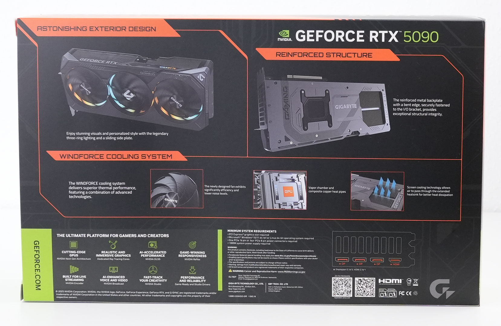
With the GeForce RTX 5090 Gaming OC, Gigabyte introduces the latest generation of its WindForce 3X cooling solution, and its 100 mm axial flow fans that ventilate two large aluminium fin stacks that pull heat form the GPU and memory via a vapor chamber plate. The card comes with a fairly high factory overclock of 2550 MHz boost compared to 2407 MHz reference. The card offers dual-BIOS, with its Silent BIOS sticking to these speeds at a more tightened fan-curve. Gigabyte is pricing the RTX 5090 Gaming OC at $2,350, a 17.5% premium over the NVIDIA baseline.
| Price | Cores | ROPs | Core Clock | Boost Clock | Memory Clock | GPU | Transistors | Memory | |
|---|---|---|---|---|---|---|---|---|---|
| RTX 3080 | $420 | 8704 | 96 | 1440 MHz | 1710 MHz | 1188 MHz | GA102 | 28000M | 10 GB, GDDR6X, 320-bit |
| RTX 4070 | $490 | 5888 | 64 | 1920 MHz | 2475 MHz | 1313 MHz | AD104 | 35800M | 12 GB, GDDR6X, 192-bit |
| RX 7800 XT | $440 | 3840 | 96 | 2124 MHz | 2430 MHz | 2425 MHz | Navi 32 | 28100M | 16 GB, GDDR6, 256-bit |
| RX 6900 XT | $450 | 5120 | 128 | 2015 MHz | 2250 MHz | 2000 MHz | Navi 21 | 26800M | 16 GB, GDDR6, 256-bit |
| RX 6950 XT | $630 | 5120 | 128 | 2100 MHz | 2310 MHz | 2250 MHz | Navi 21 | 26800M | 16 GB, GDDR6, 256-bit |
| RTX 3090 | $900 | 10496 | 112 | 1395 MHz | 1695 MHz | 1219 MHz | GA102 | 28000M | 24 GB, GDDR6X, 384-bit |
| RTX 4070 Super | $590 | 7168 | 80 | 1980 MHz | 2475 MHz | 1313 MHz | AD104 | 35800M | 12 GB, GDDR6X, 192-bit |
| RX 7900 GRE | $530 | 5120 | 160 | 1880 MHz | 2245 MHz | 2250 MHz | Navi 31 | 57700M | 16 GB, GDDR6, 256-bit |
| RTX 4070 Ti | $700 | 7680 | 80 | 2310 MHz | 2610 MHz | 1313 MHz | AD104 | 35800M | 12 GB, GDDR6X, 192-bit |
| RTX 4070 Ti Super | $750 | 8448 | 112 | 2340 MHz | 2610 MHz | 1313 MHz | AD103 | 45900M | 16 GB, GDDR6X, 256-bit |
| RX 7900 XT | $620 | 5376 | 192 | 2000 MHz | 2400 MHz | 2500 MHz | Navi 31 | 57700M | 20 GB, GDDR6, 320-bit |
| RTX 3090 Ti | $1000 | 10752 | 112 | 1560 MHz | 1950 MHz | 1313 MHz | GA102 | 28000M | 24 GB, GDDR6X, 384-bit |
| RTX 4080 | $940 | 9728 | 112 | 2205 MHz | 2505 MHz | 1400 MHz | AD103 | 45900M | 16 GB, GDDR6X, 256-bit |
| RTX 4080 Super | $990 | 10240 | 112 | 2295 MHz | 2550 MHz | 1438 MHz | AD103 | 45900M | 16 GB, GDDR6X, 256-bit |
| RX 7900 XTX | $820 | 6144 | 192 | 2300 MHz | 2500 MHz | 2500 MHz | Navi 31 | 57700M | 24 GB, GDDR6, 384-bit |
| RTX 5080 | $1000 | 10752 | 112 | 2295 MHz | 2617 MHz | 1875 MHz | GB203 | 45600M | 16 GB, GDDR7, 256-bit |
| RTX 4090 | $2400 | 16384 | 176 | 2235 MHz | 2520 MHz | 1313 MHz | AD102 | 76300M | 24 GB, GDDR6X, 384-bit |
| RTX 5090 | $2000 | 21760 | 176 | 2017 MHz | 2407 MHz | 1750 MHz | GB202 | 92200M | 32 GB, GDDR7, 512-bit |
| Gigabyte RTX 5090 Gaming OC | $2350 | 21760 | 176 | 2017 MHz | 2550 MHz | 1750 MHz | GB202 | 92200M | 32 GB, GDDR7, 512-bit |
Packaging
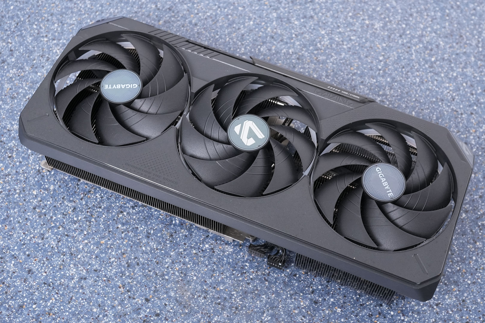
The Card
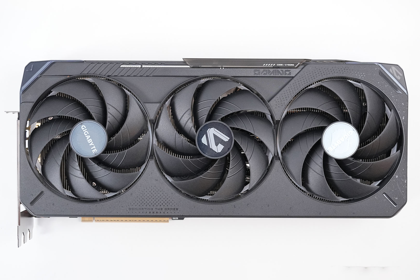
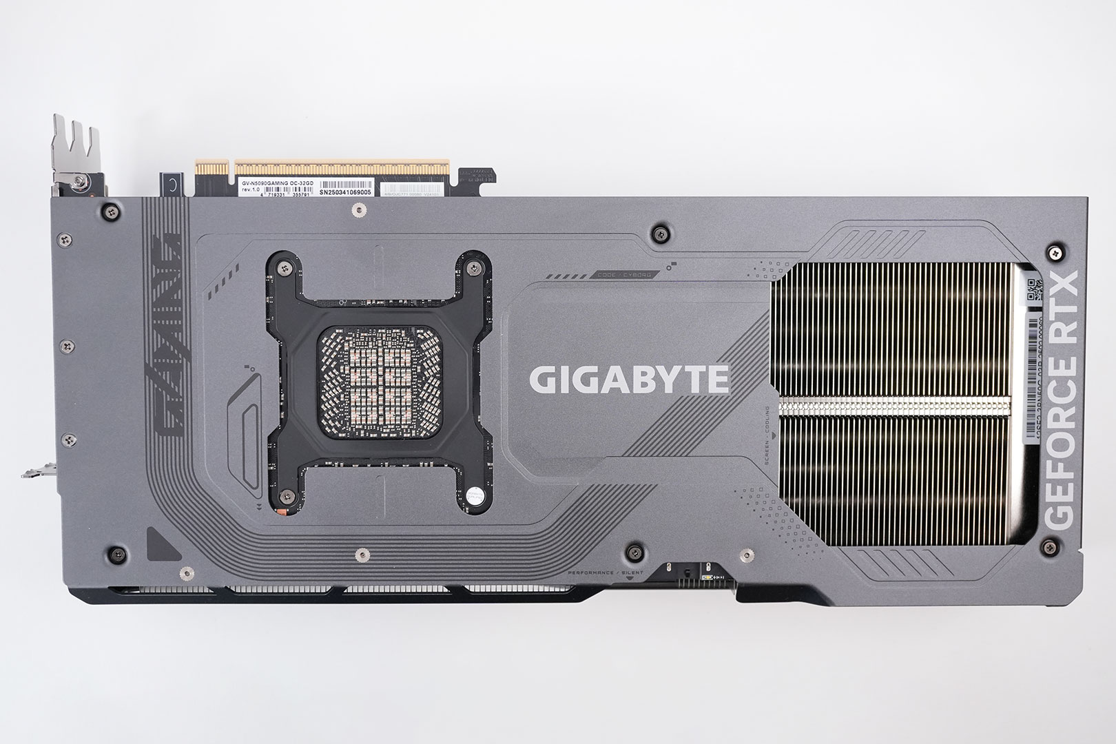
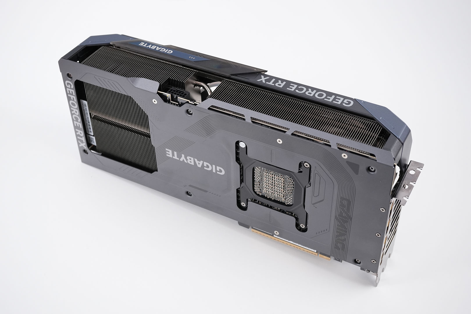
Visually, the Gigabyte RTX 5090 Gaming OC looks very similar to previous generation cards from the company, the main color theme is gray with various highlights. On the back you get a metal backplate with a large cutout.
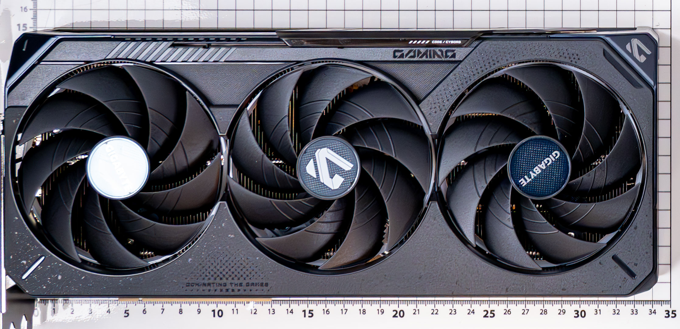
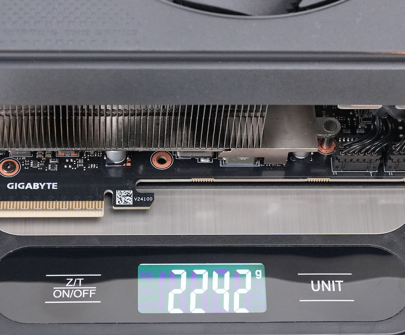
Dimensions of the card are 34.0 x 15.0 cm, and it weighs 2242 g.
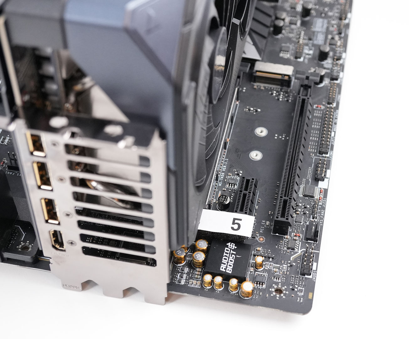
Installation requires four slots in your system. We measured the card's width to be 70 mm.
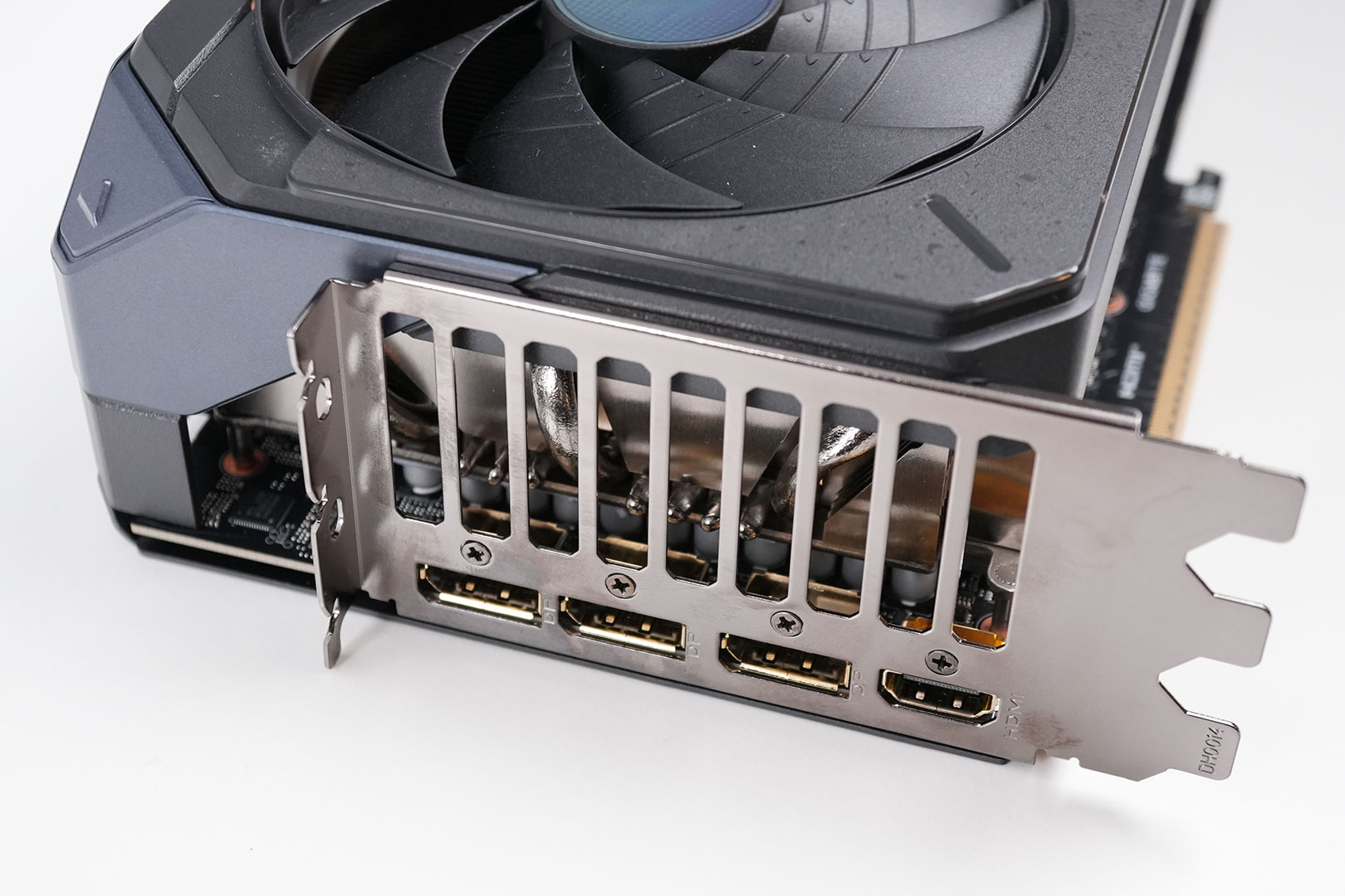
Display connectivity includes three standard DisplayPort 2.1b and one HDMI 2.1b.
Standard for all GeForce RTX 50-series Blackwell cards is a new display engine that supports three DisplayPort 2.1b outputs, each capable of UHBR20; and one HDMI 2.1a. Both interfaces support DSC (display stream compression). With DSC enabled, a single DisplayPort on this card can drive 4K 12-bit HDR at 480 Hz; or 8K 12-bit HDR at up to 165 Hz. The RTX 5090 features an updated media acceleration engine with support for 4:2:2 video formats, AV1 UHQ, and MV-HEVC. There are three independent NVENC units, and two NVDEC.
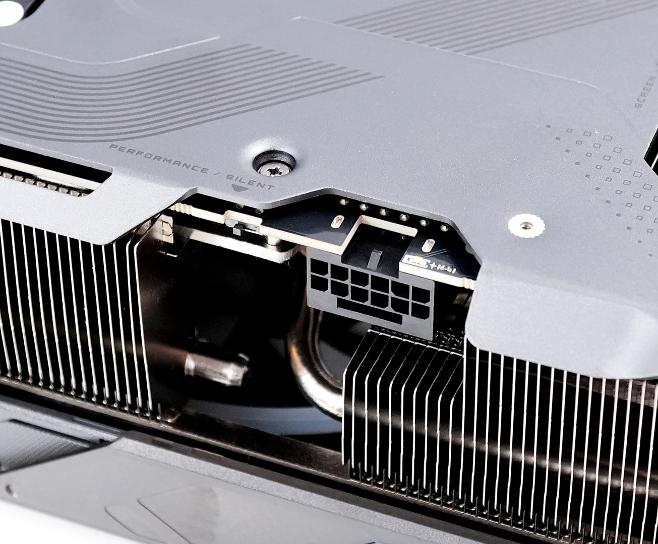
The card uses a single 16-pin connector, which allows a maximum power draw of 600 W.
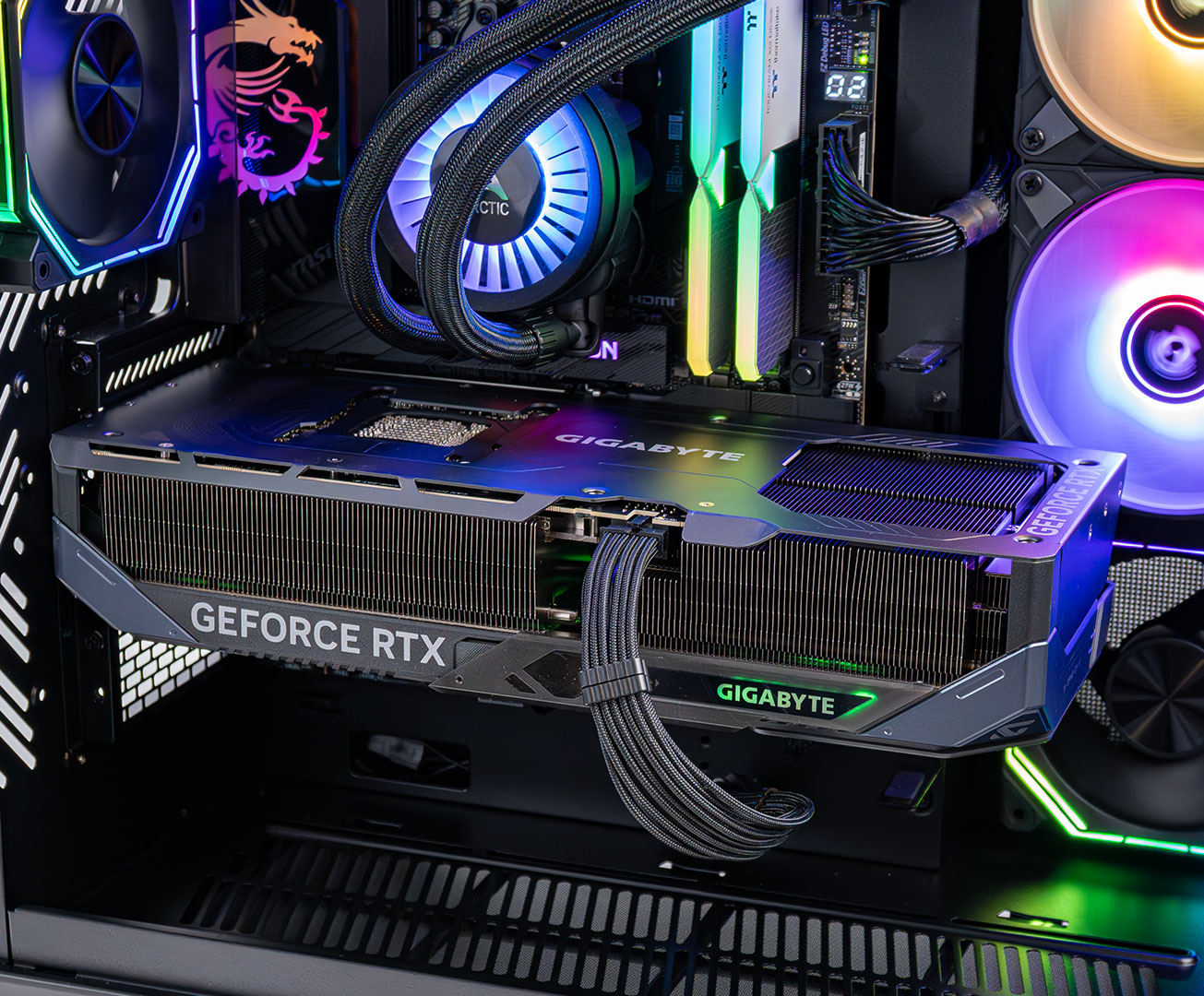
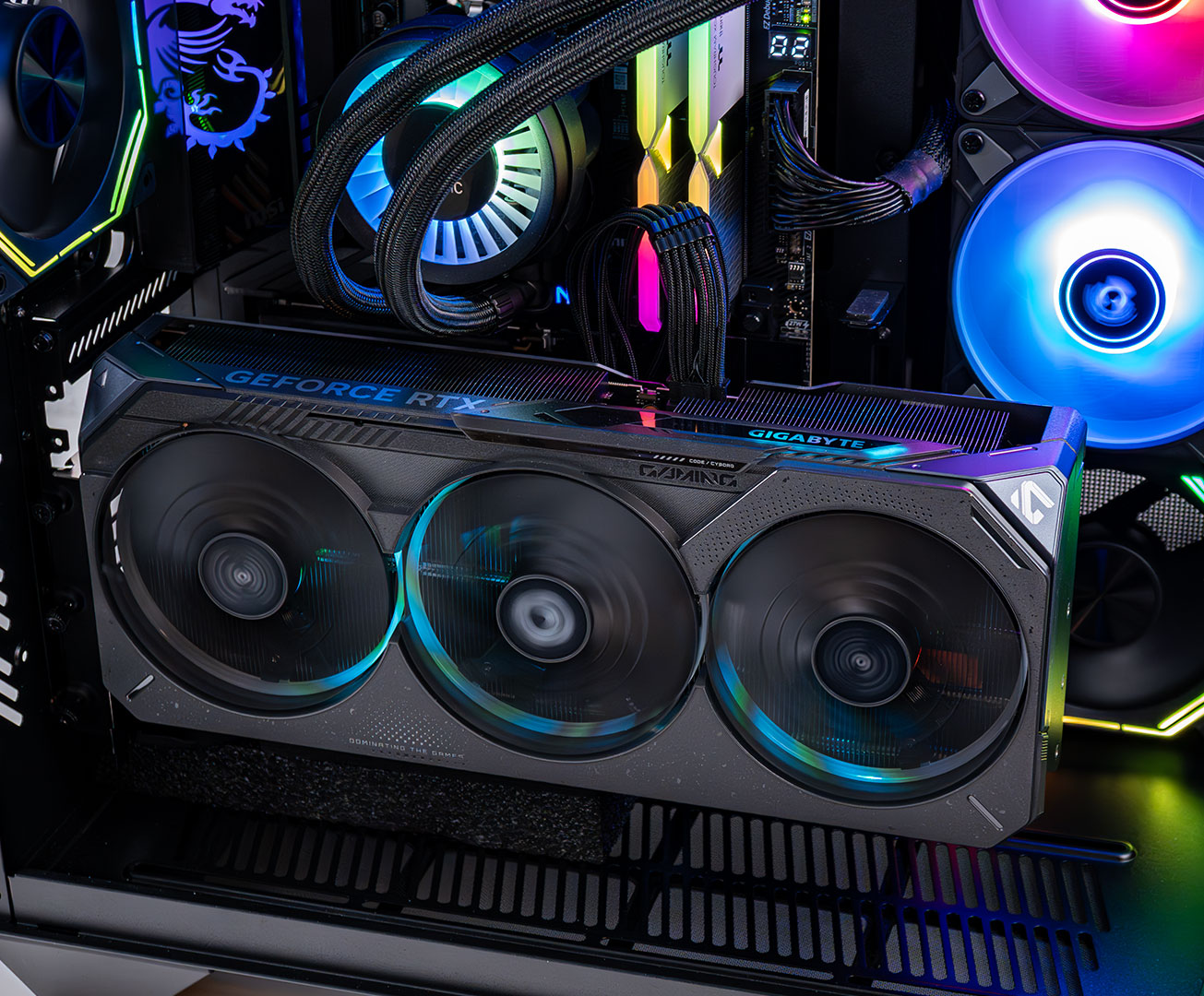
Gigabyte has added RGB illumination zone on the logo and behind the three fans.
Teardown
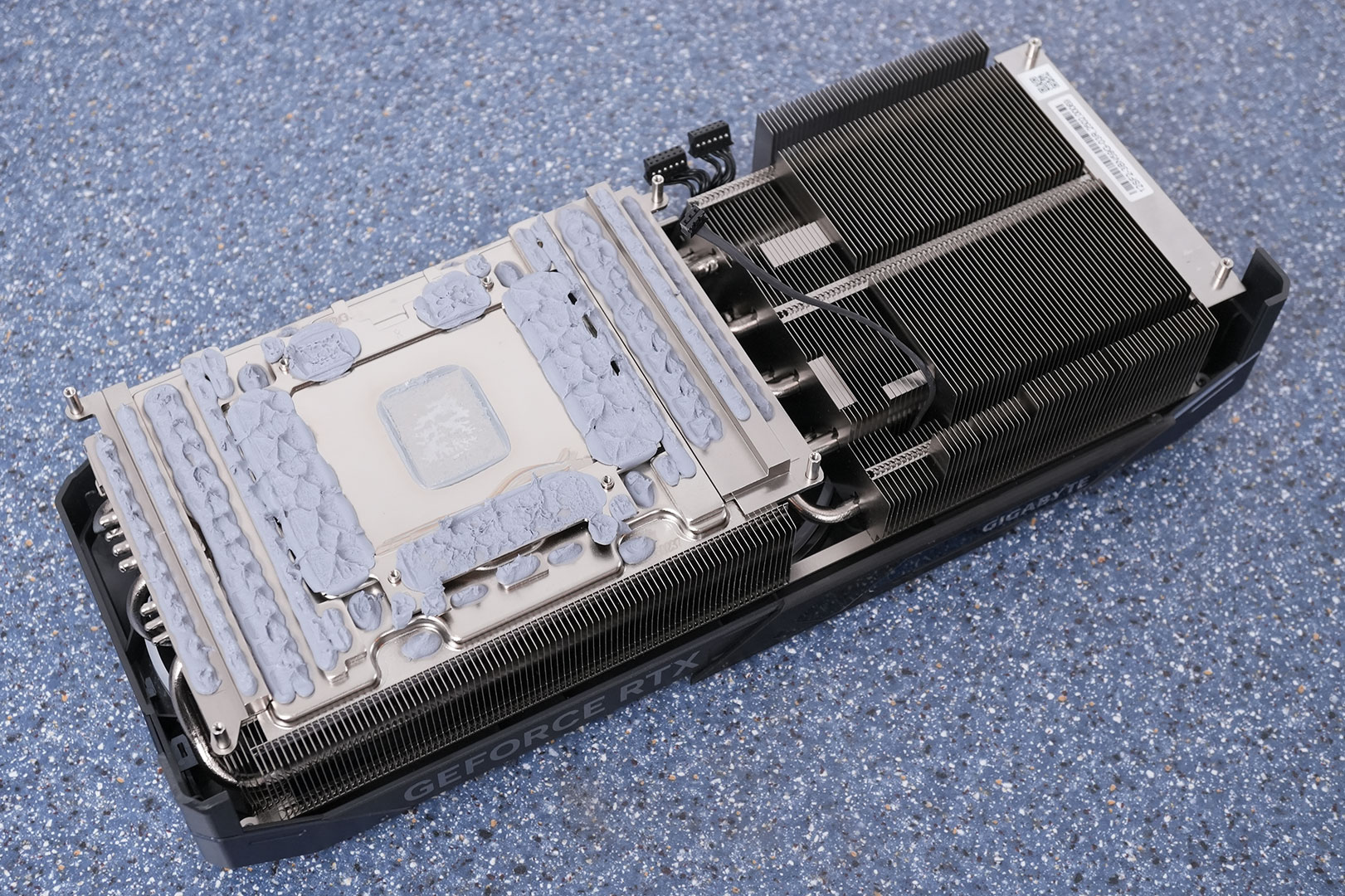
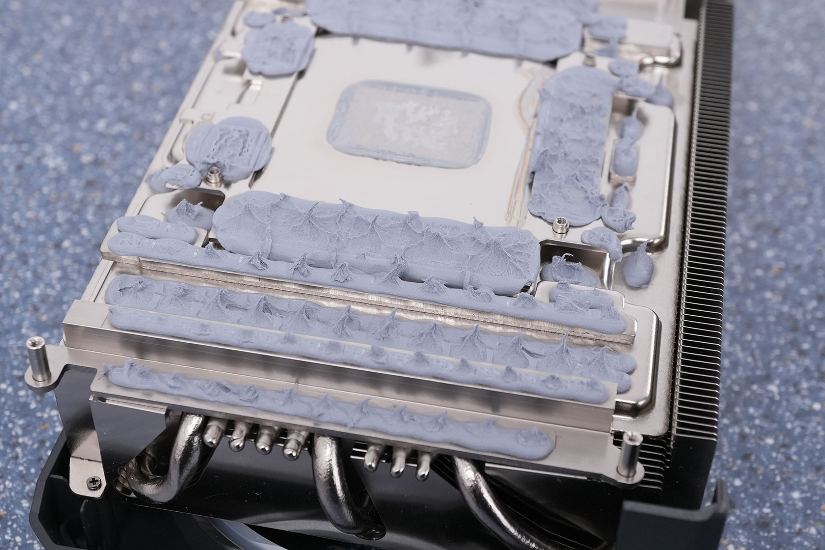
Gigabyte's thermal solution uses eight heatpipes and a vapor-chamber. It provides cooling not only for the GPU, but also for the memory chips and VRM circuitry. Note the use of thermal putty instead of thermal pads, which makes maintenance hard, because you'll probably have to replace everything every time you take the card apart.
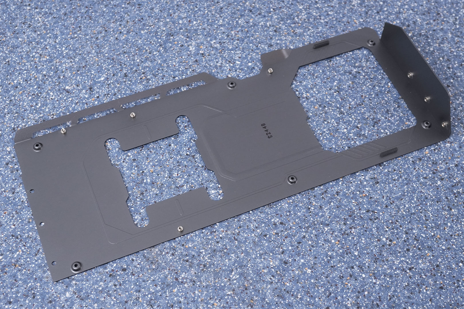

The backplate protects the card against damage during installation and handling.
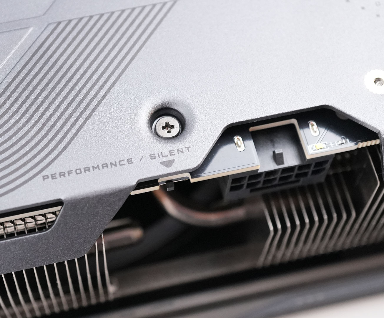
This BIOS switch lets you select between the default "Performance" BIOS and a "Quiet" BIOS that runs a more relaxed fan curve.
High-resolution PCB Pictures
These pictures are for the convenience of volt modders and people who would like to see all the finer details on the PCB. Feel free to link back to us and use these in your articles, videos or forum posts.
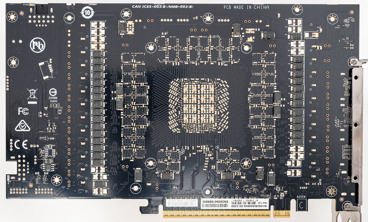
High-resolution versions are also available (front, back).
Circuit Board (PCB) Analysis

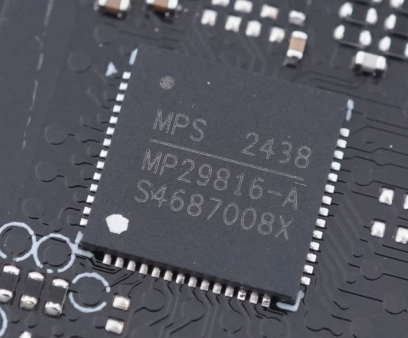
A 22-phase VRM powers the GPU, highlighted in the red rectangles above. These are controlled by a Monolithic Power Systems MP29816 controller.

All GPU power phases use Monolithic MPS MP87993 DrMOS with a rating of 50 A.
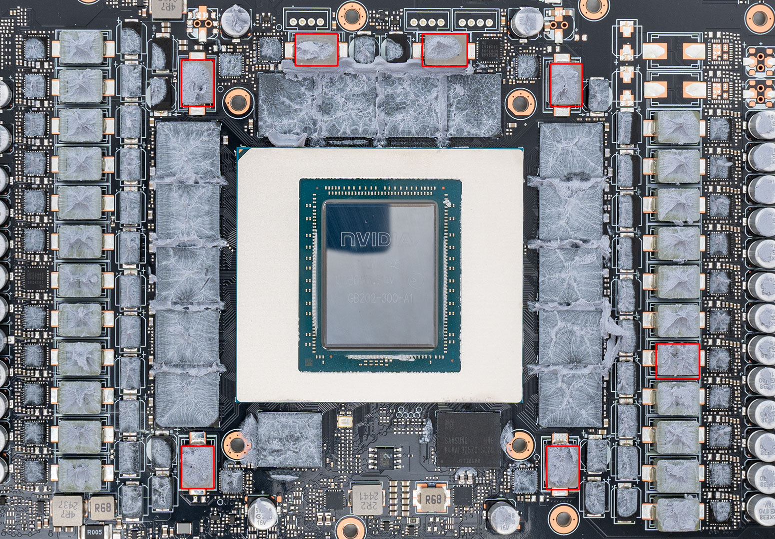

Powering the eight GDDR7 memory chips is a 7-phase VRM driven by a Monolithic MP2988 controller (this variant uses a smaller package).

Just like GPU, the memory is handled by Monolithic MP87993 DrMOS chips.
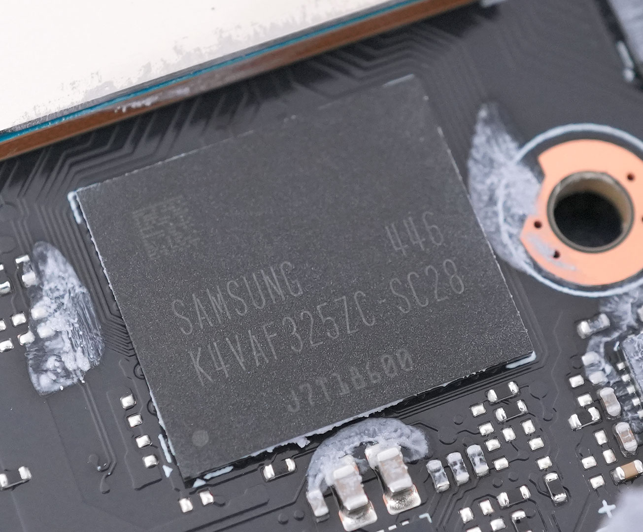
The GDDR7 memory chips are made by Samsung, and bear the model number K4VAF325ZC-SC28, they are rated for 28 Gbps.
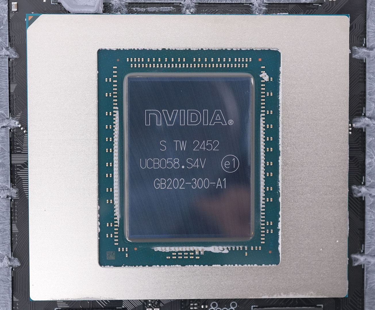
The NVIDIA GB202 GPU at the heart of the GeForce RTX 5090 is massive. It is fabricated using a 5 nanometer "NVIDIA 4N" process at TSMC Taiwan (same process as Ada). The die measures 750 mm², and comes with a transistor count of 92.2 billion.
Test System
| Test System - GPU 2025.1 | |
|---|---|
| Processor: | AMD Ryzen 7 9800X3D Zen 5, 5.2 GHz, 8 cores / 16 threads |
| Motherboard: | MSI X870E Carbon Wi-Fi BIOS 7E49v1A15 |
| Resizable BAR: | Enabled on all supported cards (NVIDIA, AMD & Intel) |
| Memory: | Thermaltake TOUGHRAM XG 2x 16 GB DDR5-6200 MHz 28-36-36-76 UCLK 1:1 |
| Cooling: | Arctic Liquid Freezer III 280 mm AIO |
| Thermal Paste: | Arctic MX-6 |
| Storage: | 4 TB M.2 NVMe SSD |
| Power Supply: | Seasonic Focus GX 1000 W ATX 3.0 / 16-pin 12VHPWR |
| Case: | darkFlash DY470 |
| Operating System: | Windows 11 Professional 64-bit 24H2 VBS enabled (Windows 11 default) |
| Drivers: | RTX 5080: 572.12 Press Driver RTX 5090: 571.86 Press Driver NVIDIA: 566.14 WHQL AMD: 24.10.1 WHQL Intel: 101.6314 WHQL Arc B580: 101.6256 Press Driver Date of Retest |


- All games and cards are tested with the drivers listed above—no performance results were recycled between test systems. Only this exact system with exactly the same configuration is used for all results in this review.
- All graphics cards are tested using the same game version.
- All games are set to their highest quality setting unless indicated otherwise.
- All games are running at their native resolution without upscaling (no DLSS or FSR), except for the results on the "DLSS 4" page where we specifically look into that feature's performance
- All games have ray tracing disabled, except for testing on the "Ray Tracing" page
- AA and AF are applied via in-game settings, not via the driver's control panel.
- Before starting measurements, we heat up the card for each test to ensure a steady state is tested. This ensures that the card won't boost to unrealistically high clocks for only a few seconds until it heats up, as that doesn't represent prolonged gameplay.
- For better real-life applicability, all game tests use custom in-game test scenes, not the integrated benchmarks
- All cards used for comparison are reference designs. When a reference design does not exist, we go the extra mile and buy the closest possible match, using reference clocks and default power limit.
- 1920x1080: Most popular monitor resolution.
- 2560x1440: Intermediary resolution between Full HD and 4K, with reasonable performance requirements.
- 3840x2160: 4K Ultra HD resolution, available on high-end monitors.
Our Patreon Silver Supporters can read articles in single-page format.
Mar 25th, 2025 14:38 EDT
change timezone
Latest GPU Drivers
New Forum Posts
- TPU's Nostalgic Hardware Club (20122)
- Did Nvidia purposely gimp the performance of 50xx series cards with drivers (4)
- Windows 10 Vs 11, Which one too choose? (99)
- HalfLife2 RTX Demo Is out! (313)
- What are you playing? (23263)
- Do you use Linux? (545)
- Help the experts to explain what this is? (14)
- What is going to be your next tech upgrade? just curious :) (5)
- Is RX 9070 VRAM temperature regular value or hotspot? (190)
- Undervolting 13th Gen Intel(R) Core(TM) i7-13650HX ROG Strix G16 (5)
Popular Reviews
- Assassin's Creed Shadows Performance Benchmark Review - 30 GPUs Compared
- be quiet! Pure Rock Pro 3 Black Review
- ASUS ProArt X870E-Creator Wi-Fi Review
- ASRock Radeon RX 9070 XT Taichi OC Review - Excellent Cooling
- Sapphire Radeon RX 9070 XT Nitro+ Review - Beating NVIDIA
- ASUS GeForce RTX 5070 TUF OC Review
- AMD Ryzen 9 9950X3D Review - Great for Gaming and Productivity
- Quick Look: Jelly Key Mystic Snake Artisan Keycaps
- AMD Ryzen 7 9800X3D Review - The Best Gaming Processor
- XFX Radeon RX 9070 XT Mercury OC Magnetic Air Review
Controversial News Posts
- AMD RDNA 4 and Radeon RX 9070 Series Unveiled: $549 & $599 (260)
- AMD Radeon RX 9070-series Pricing Leaks Courtesy of MicroCenter (158)
- MSI Doesn't Plan Radeon RX 9000 Series GPUs, Skips AMD RDNA 4 Generation Entirely (142)
- Microsoft Introduces Copilot for Gaming (123)
- AMD Radeon RX 9070 XT Reportedly Outperforms RTX 5080 Through Undervolting (118)
- NVIDIA Reportedly Prepares GeForce RTX 5060 and RTX 5060 Ti Unveil Tomorrow (115)
- Over 200,000 Sold Radeon RX 9070 and RX 9070 XT GPUs? AMD Says No Number was Given (100)
- NVIDIA GeForce RTX 5050, RTX 5060, and RTX 5060 Ti Specifications Leak (96)