 99
99
Intel Core i9-7900X 3.3 GHz Review
Test Setup »Architecture
At the heart of the Core i9-7900X is the new "Skylake-X" silicon, which makes up the bulk of Intel's Core X processor family. This is a die built on the 14 nm+ silicon fabrication process, and it comes in three principal variants, Skylake-X LCC (low core-count), Skylake-X HCC (high core-count), and Skylake-X XCC (extreme core-count). The LCC die physically only has 10 CPU cores, while the HCC die physically has 18 cores, and the XCC die has 28 cores. The Core i7-7800X, i7-7820X, and i9-7900X are based on the LCC die; while higher Core i9 12-core, 14-core, 16-core, and 18-core models are based on the HCC die. The 28-core XCC die has an extra pair of DDR4 memory controllers and is found on certain Xeon Scalable models. Intel hasn't implemented it on the client platform yet.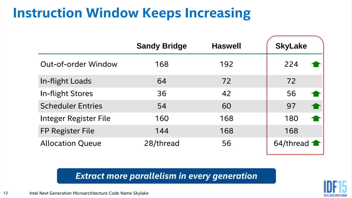
As we mentioned in the previous page, the LGA2066 package consists of a "double-decked" fiberglass substrate. The bottom substrate has the LGA contact points and some common electrical components, while the upper substrate is bumped to the CPU die above and soldered to the bottom substrate via a ball-grid array (BGA) below. This substrate can pack wiring of extremely high density. The double-decked approach gives the LGA2066 package a degree of modularity as Intel is juggling four dies on it - Skylake-X LCC, Skylake-X HCC, Skylake-X XCC, and the quad-core Kaby Lake-X.


The Core i9-7900X is a 10-core processor, with HyperThreading enabling 20 logical CPUs (threads) for your operating system to deal with. These CPU cores are based on Intel's "Skylake" micro-architecture, which has dominated Intel's CPU lineup since 2015. Each CPU core on this processor has 1 MB of dedicated L2 cache, while the cores share 13.75 MB of L3 cache (1,408 KB LLC segment per core). There are two integrated 128-bit DDR4 memory controllers, and these drive the processor's quad-channel memory interface. This model is endowed with the full PCI-Express gen 3.0 lane budget of the silicon for 44 PCI-Express lanes. That's enough to drive up to two graphics cards at full x16 bandwidth, besides the rest of the platform.
Mesh On-Die Interconnect
Since building "Nehalem," its first monolithic quad-core die, Intel has used the "Ring Bus" interconnect to handle high-bandwidth communications between the various components on the die, i.e., the CPU cores, integrated northbridge, integrated graphics (if any), etc. This is a sort of serial interconnect in which data is collected and dispatched in a similar fashion to an old-school ring-topology coaxial LAN, with each enabled component marking a "ring stop."
Over the years, Intel has made the ring bus broader to keep up with the increasing performance of the cores and more memory (data) flowing through it; but as Intel kept piling up the core count (ring stops), its processor designers found themselves in a situation where the Ring Bus inflicts an intolerable amount of latency for inter-core communication on processors with large core counts. It needed a new on-die interconnect to address this. Enter the Mesh Interconnect.
Originally developed for the "Knights Landing" super-scalar compute processor that features dozens of compute elements, the Mesh Interconnect is a deployment of multiple Ring Bus stops per component that progress in different directions, linking up with different components. Each on-die component, be it a CPU core, the memory controller, integrated-northbridge, etc., now has multiple Ring Bus terminals, which creates multiple Ring Bus paths crisscrossing the die, like a mesh. This approach significantly brings down inter-core communication latency and provides Intel with a means to scale up core counts.
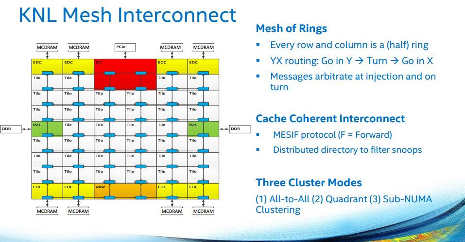
Cache Hierarchy Revision
The other major change Intel introduced with the "Skylake-X" silicon is a redesigned cache hierarchy. Since "Nehalem," Intel has used an arbitrary 256-kilobyte dedicated L2 cache per core on its multi-core processors and up to 2 MB of shared L3 cache per core (i.e. a 4-core chip has up to 8 MB L3 cache, an 8-core chip has 16 MB, etc.). The company seems to have understood that today's multi-threaded workloads don't require as much shared on-die cache, and that it would be prudent to bolster the faster and dedicated L2 caches to increase per-core performance, and to locally pool more data in a high core-count environment, particularly when it takes several ring hops to reach the memory controller.
Intel has thus increased the dedicated L2 cache size to 1 MB per core (a four-fold increase from the previous generation), while decreasing the shared L3 cache per core to roughly 1.375 MB/core (i.e. a 10-core chip has 13.75 MB, a 16-core chip has 22 MB, etc.)
Turbo Boost Max 3.0 Technology
The third major change introduced with "Skylake-X" is the Turbo Boost Max 3.0 technology. It's a reworked Turbo Boost algorithm that allocates less-parallelized workload to a core identified on-the-fly as the "best core" on parameters such as lowest temperature, lowest cache allocation, fewest mesh hops to the memory controllers or uncore, etc., and elevates it to the highest boost C-state, which is usually 200 MHz higher than the advertised max boost clock-speed. Other cores, if required, are progressively boosted as they're graded on those parameters. This is unlike rival AMD's XFR (extended frequency range), which is a 50-200 MHz boost if the cores are able to stay below a temperature threshold and aren't heating up quickly enough (i.e. if your cooling is effective enough).
The X299 Platform
Intel launched its Core X processors alongside the X299 Express chipset. By itself, X299 has a similar feature-set to the Z270 Express, minus the onboard graphics. It puts out 24 PCI-Express gen 3.0 general-purpose lanes of its own, has a 6-port SATA 6 Gbps SATA RAID controller, two GbE MACs, and an integrated USB 3.1 controller. Whatever surplus M.2 slots, U.2 ports, PCIe slots, etc., you see on this platform versus the mainstream Z270 platform is due to the PCI-Express lanes coming from the LGA2066 processors.
Intel Core i7-7800X and i7-7820X feature a 28-lane PCI-Express root complex that drives just one graphics card at full x16 bandwidth. Additional graphics cards have to eat into its lane budget using 3-way lane switches. The Core i9 family, on the other hand, features the fully unlocked 44-lane PCI-Express root complex, which means you can drive up to two graphics cards at x16 bandwidth and are ready for 3-way/4-way multi-GPU. The added lane budget also lets you add more high-bandwidth devices, such as 10 GbE adapters, Thunderbolt cards, PCIe SSDs, etc.
Jun 30th, 2025 21:33 CDT
change timezone
Latest GPU Drivers
New Forum Posts
- Post your Cinebench 2024 score (657)
- Laptop overclocking adventures (1238)
- [INTEL]-How To Update Your Microcode for Intel HX 13/14th Gen. CPUs Laptops/Mobile Easily. (172)
- Will you buy a RTX 5090? (584)
- The TPU UK Clubhouse (26530)
- Optane and "enable write caching " (27)
- Question about Intel Optane SSDs (87)
- Do you use Linux? (664)
- Remember Fermi? Well here's my EVGA GTX 480 that I picked up for just 19 Euros! (9)
- Vega owners club (587)
Popular Reviews
- ASUS ROG Crosshair X870E Extreme Review
- Sapphire Radeon RX 9060 XT Pulse OC 16 GB Review - Samsung Memory Tested
- AVerMedia CamStream 4K Review
- Lexar NQ780 4 TB Review
- AMD Ryzen 7 9800X3D Review - The Best Gaming Processor
- Upcoming Hardware Launches 2025 (Updated May 2025)
- Sapphire Radeon RX 9070 XT Nitro+ Review - Beating NVIDIA
- AMD Ryzen 9 9950X3D Review - Great for Gaming and Productivity
- NVIDIA GeForce RTX 5060 8 GB Review
- ASRock Phantom Gaming Z890 Riptide Wi-Fi Review
TPU on YouTube
Controversial News Posts
- Intel's Core Ultra 7 265K and 265KF CPUs Dip Below $250 (288)
- NVIDIA Grabs Market Share, AMD Loses Ground, and Intel Disappears in Latest dGPU Update (204)
- Some Intel Nova Lake CPUs Rumored to Challenge AMD's 3D V-Cache in Desktop Gaming (140)
- NVIDIA Launches GeForce RTX 5050 for Desktops and Laptops, Starts at $249 (105)
- Microsoft Partners with AMD for Next-gen Xbox Hardware (105)
- Intel "Nova Lake‑S" Series: Seven SKUs, Up to 52 Cores and 150 W TDP (100)
- NVIDIA GeForce RTX 5080 SUPER Could Feature 24 GB Memory, Increased Power Limits (94)
- Reviewers Bemused by Restrictive Sampling of RX 9060 XT 8 GB Cards (88)