 55
55
Ivy Bridge PCI-Express Scaling with HD 7970 and GTX 680 Review
Test Setup »Introduction

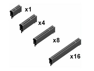
The last time we did an article on PCI-Express scaling, was when graphics cards were finally able to saturate the bandwidth of PCI-Express x16. Not only was it a time when PCI-Express 2.0 was prevalent, but also when the first DirectX 11 GPU hit the market, and that was over six years into the introduction of the PCI-Express bus interface. Since 2009, thanks to fierce competition between NVIDIA and AMD, GPU performance levels have risen at a faster rate than ever, and the latest generation of high-end GPUs launched by the two GPU rivals adds support for the new PCI-Express 3.0 interface. The new interface sprung new questions from users like "Do I need a new motherboard to run a PCI-Express 3.0 card?", "Will my new PCI-Express 3.0 card be much slower on an older motherboard?" or "My motherboard supports only x8 for multiple cards, will performance suck?"
The industry's first PCI-Express 8 GT/s-capable platform was released last year, with Intel's Sandy Bridge-E. SB-E isn't officially PCI-Express 3.0-certified; while AMD Southern Islands GPUs can function in PCI-Express 3.0 on the platform, NVIDIA's GeForce Kepler family of GPUs, so far, can't. The 22 nm Core processor family, codenamed Ivy Bridge, however, settles the issue by providing a PCI-Express 3.0-certified root-complex, and GPUs from both sides of the fence are tested to work on the new mode. PCI-Express 3.0 close to doubles the data bandwidth available to a connected device, per lane.

While PCI-Express 1.0 pushes 250 MB/s per direction, PCI-Express 2.0 pushes 500 MB/s, and PCI-Express 3.0 doubles that to 1 GB/s. While the resulting absolute bandwidth of PCI-Express 3.0 x16, 32 GB/s, might seem overkill, the ability to push that much data per lane could come to the rescue of configurations such as 8-lanes (x8) and 4-lanes (x4). Another impressive feature of Ivy Bridge Core processors, provided they're paired with Intel Z77 Express chipset, is that the second x8 link from the CPU root complex can be split as two x4 links, making x8/x4/x4 possible, giving some motherboards 3-way SLI and CrossFireX capabilities without clogging the DMI chipset bus (that 4 GB/s pipe between the CPU and chipset), which is better left untouched by graphics cards to help with today's bandwidth-hungry SSDs.

In this review, we test the impact of running the AMD Radeon HD 7970 and the GeForce GTX 680 on Intel Ivy Bridge PCI-Express slots that are electrically PCI-Express x16, x8 and x4. We tested all three generations of the PCI-Express interface: 1.1, 2.0 and 3.0.
This review is made possible thanks to an awesome BIOS option given to us by ASUS ROG Maximus V Gene motherboard, which allows us to toggle the CPU's PCI-Express root complex between PCI-Express 1.0, 2.0, and 3.0 modes. To modify the number of lanes available to the GPU, we used common plastic adhesive tape.
For your reference, we wrote similar articles in the past: GTX 480 PCIe Scaling, HD 5870 PCIe Scaling.
Apr 26th, 2025 09:23 EDT
change timezone
Latest GPU Drivers
New Forum Posts
- Are the 8 GB cards worth it? (248)
- I dont understand the phone OS world..... (97)
- Whats your favourite Linux Distro? (231)
- (Some of) What I'd like to See From a Final Fantasy IX Remake (42)
- pc randomly blackscreening (10)
- Companies should be called out for this (96)
- Arrow Lake Z890 board + RAM (1)
- Oblivion Remastered (25)
- Can GPU-z shows effective core clocks (RTX 5000 v/f curve) ? (0)
- What are you playing? (23469)
Popular Reviews
- NVIDIA GeForce RTX 5060 Ti 8 GB Review - So Many Compromises
- Clair Obscur: Expedition 33 Performance Benchmark Review - 33 GPUs Tested
- Crucial CUDIMM DDR5-6400 128 GB CL52 Review
- Colorful iGame B860M Ultra V20 Review
- Oblivion Remastered Handheld Performance Review
- Upcoming Hardware Launches 2025 (Updated Apr 2025)
- Sapphire Radeon RX 9070 XT Pulse Review
- Sapphire Radeon RX 9070 XT Nitro+ Review - Beating NVIDIA
- AMD Ryzen 7 9800X3D Review - The Best Gaming Processor
- ASUS GeForce RTX 5060 Ti TUF OC 16 GB Review
Controversial News Posts
- NVIDIA GeForce RTX 5060 Ti 16 GB SKU Likely Launching at $499, According to Supply Chain Leak (182)
- NVIDIA Sends MSRP Numbers to Partners: GeForce RTX 5060 Ti 8 GB at $379, RTX 5060 Ti 16 GB at $429 (127)
- NVIDIA Launches GeForce RTX 5060 Series, Beginning with RTX 5060 Ti This Week (115)
- Nintendo Confirms That Switch 2 Joy-Cons Will Not Utilize Hall Effect Stick Technology (105)
- Nintendo Switch 2 Launches June 5 at $449.99 with New Hardware and Games (99)
- Sony Increases the PS5 Pricing in EMEA and ANZ by Around 25 Percent (84)
- NVIDIA PhysX and Flow Made Fully Open-Source (77)
- Parts of NVIDIA GeForce RTX 50 Series GPU PCB Reach Over 100°C: Report (75)