 24
24
MSI GeForce GTX 580 Lightning Xtreme Edition 3 GB Review
Test Setup »A Closer Look
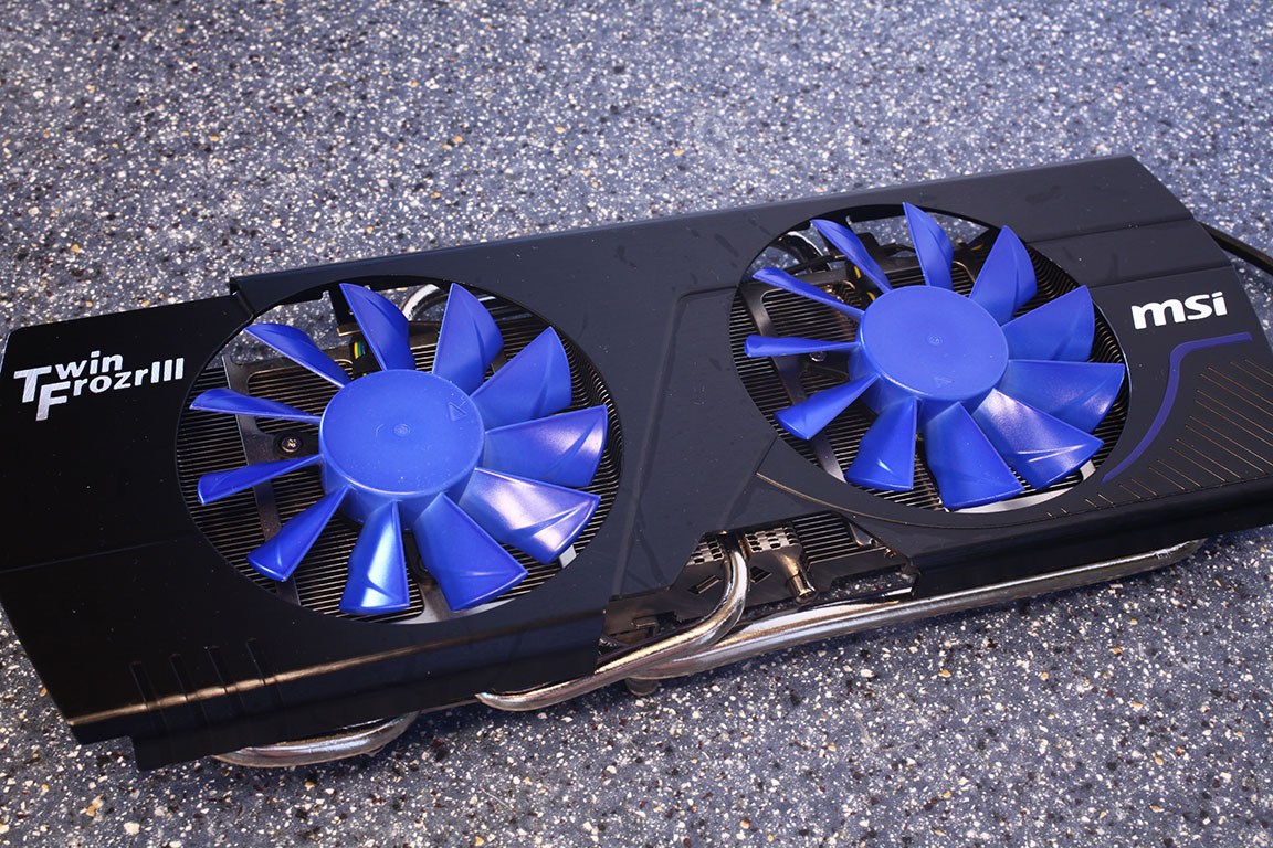
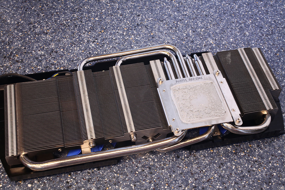
MSI's five-heatpipe cooler seems to be the same as on the normal GTX 580 Lightning with the exception of the fan blades. According to MSI they will turn white when the card overheats, I couldn't replicate that behaviour though. Also MSI has added a dust removal system which switches the fan rotation direction to minimize dust buildup.

The cards has two 8-pin PCIe power connectors. This configuration is good for up to 375 W power draw.
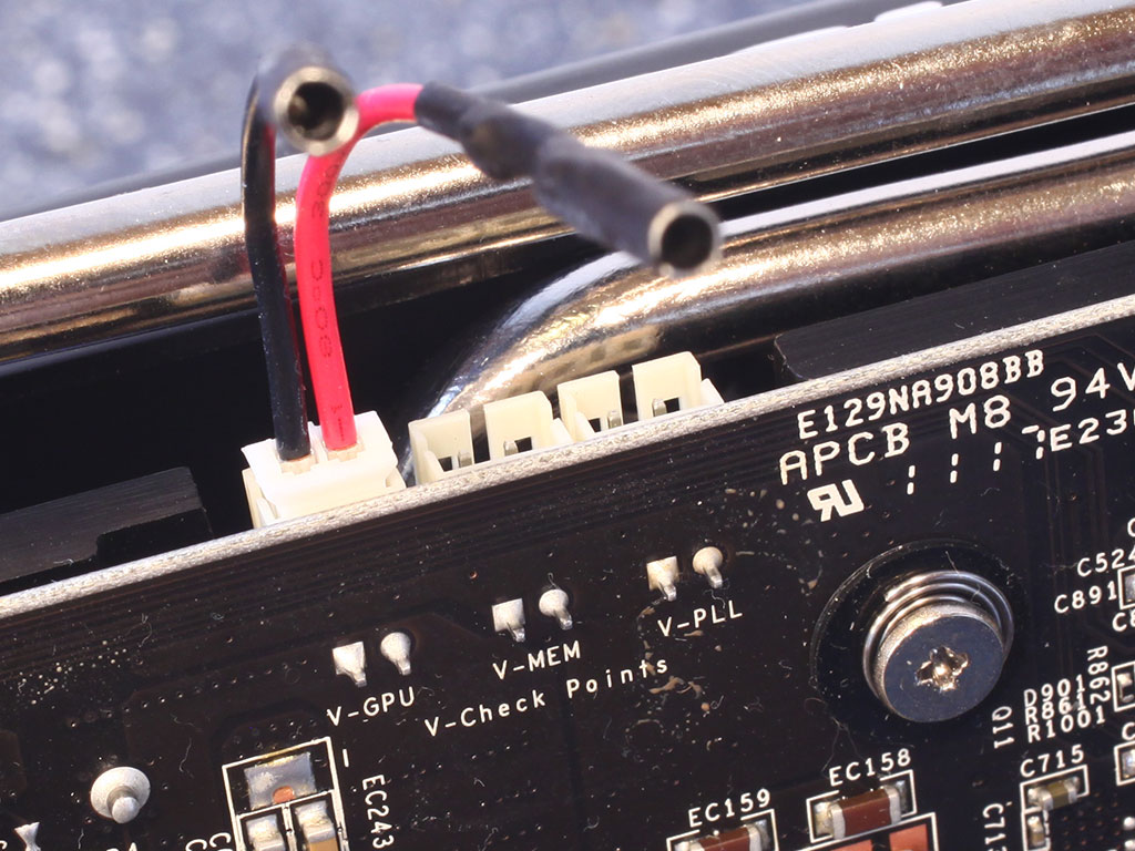
MSI has included three easy to access voltage measurement points near the top edge of the PCB. You have access to GPU Voltage, Memory Voltage and PLL Voltage. I attached one of the included measurement cables to the VGPU point to show how the system works - there are three cables included.
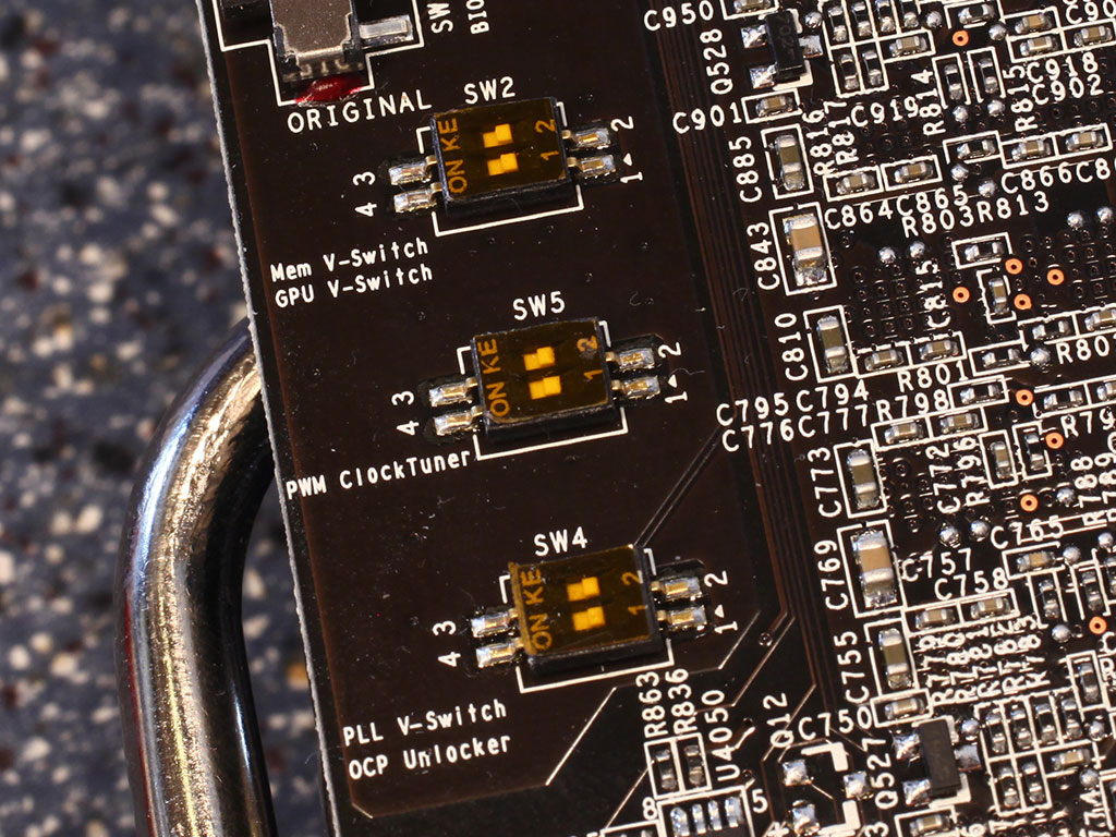
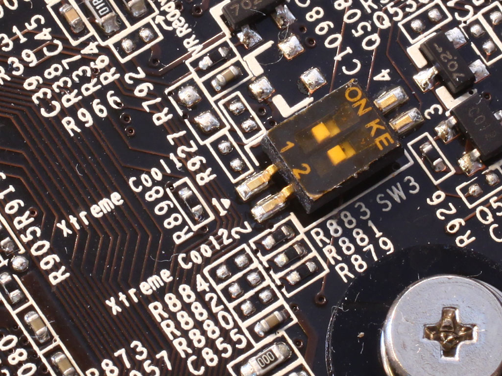
MSI has placed several DIP switches on the board for some basic non-software control of the card. Starting from the top you have Memory voltage and GPU voltage which provides an instant boost to those voltages, next we have PWM ClockTuner which lets you select the PWM clock frequency from 260 MHz to 310 MHz. Finally we have a switch to increase PLL voltage and one to remove the overcurrent protection of the card. An extra DIP switch is located near middle of the board and is used to enable several LN2 fixes which help with stability when using Liquid Nitrogen cooling.

The BIOS switch will let you select between the default BIOS and a BIOS that has no cold slowdown issue. When GPU temperature goes negative, the GPU sometimes thinks it is overheating which would cause it to reduce clock speeds. Also the second BIOS serves as a backup in case something goes wrong during a BIOS flash.
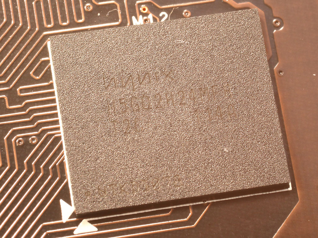
The GDDR5 memory chips are made by Hynix, and carry the model number H5GQ2H24MFR-T2C. They are specified to run at 1250MHz (5000 MHz GDDR5 effective).

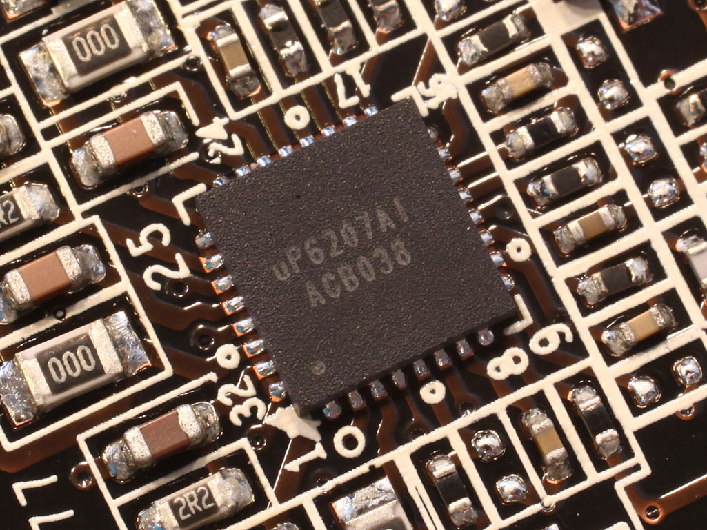
MSI has put two voltage controllers on their card to enable their triple-voltage change feature.
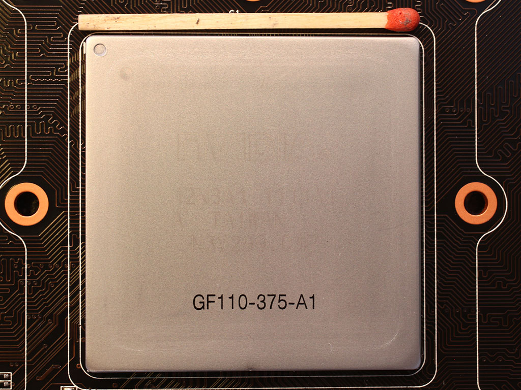
NVIDIA's GeForce 110 graphics processor is made on a 40 nm process at TSMC Taiwan. It uses approximately 3.0 billion transistors which is 200 million less than the GF100. Please note that the silvery metal surface you see is the heatspreader of the GPU. According to NVIDIA, the die size of the GF110 graphics processor is 520 mm².
Feb 2nd, 2025 13:11 EST
change timezone
Latest GPU Drivers
New Forum Posts
- Wow YouTube is a Hog (0)
- Best silent laptop for 1000 dollars max.? (0)
- Testing max ram overclock pn Ryzen 1700 (37)
- Modem/Router suggestions (15)
- Starting my AM5 build (16)
- Please let me know if the UPS that I want to buy is good or not for my PC. (118)
- eXtreme Outer Vision PSU Calculator Shutting Down :( (7)
- WHAT SHOULD I DO IF MY BD PROCHOT GREY WON'T OPEN? (1)
- QVL - Myth, Legend, Marketing/Advertising, what is your take? (71)
- ThrottleStop triggers Defender on svchost process (3)
Popular Reviews
- NVIDIA GeForce RTX 5080 Founders Edition Review
- Spider-Man 2 Performance Benchmark Review - 35 GPUs Tested
- Galax GeForce RTX 5080 1-Click OC Review
- NVIDIA DLSS 4 Transformer Review - Better Image Quality for Everyone
- MSI GeForce RTX 5080 Vanguard SOC Review
- ASUS GeForce RTX 5080 Astral OC Review
- Gigabyte GeForce RTX 5080 Gaming OC Review
- MSI GeForce RTX 5080 Suprim SOC Review
- ASUS GeForce RTX 5090 Astral OC Review - Astronomical Premium
- NVIDIA GeForce RTX 5090 Founders Edition Review - The New Flagship
Controversial News Posts
- NVIDIA 2025 International CES Keynote: Liveblog (470)
- AMD Debuts Radeon RX 9070 XT and RX 9070 Powered by RDNA 4, and FSR 4 (349)
- AMD is Taking Time with Radeon RX 9000 to Optimize Software and FSR 4 (251)
- AMD Radeon 9070 XT Rumored to Outpace RTX 5070 Ti by Almost 15% (244)
- AMD Denies Radeon RX 9070 XT $899 USD Starting Price Point Rumors (239)
- AMD Radeon RX 9070 XT & RX 9070 Custom Models In Stock at European Stores (226)
- NVIDIA GeForce RTX 5090 Features 575 W TDP, RTX 5080 Carries 360 W TDP (217)
- New Leak Reveals NVIDIA RTX 5080 Is Slower Than RTX 4090 (215)