 33
33
MSI GeForce GTX 580 Lightning 1536 MB Review
Test Setup »A Closer Look


MSI's cooler uses five heatpipes that transfer heat quickly from the GPU baseplate to the huge fin array which is cooled by two fans.

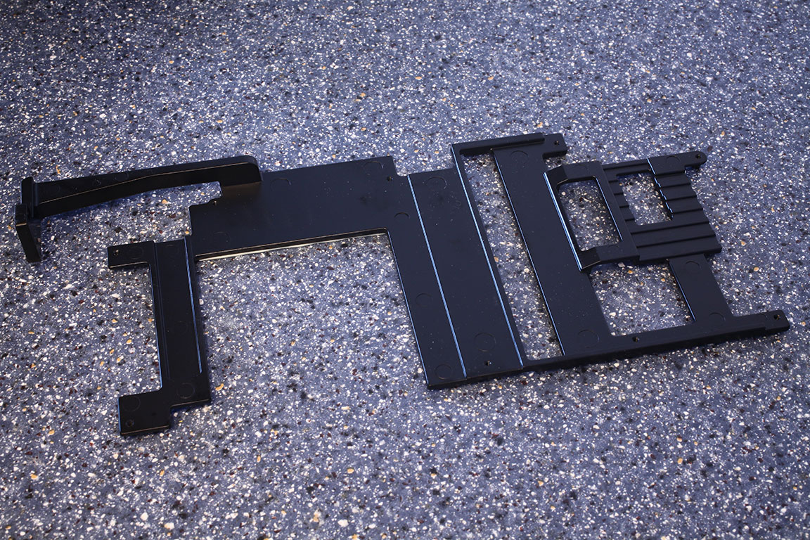
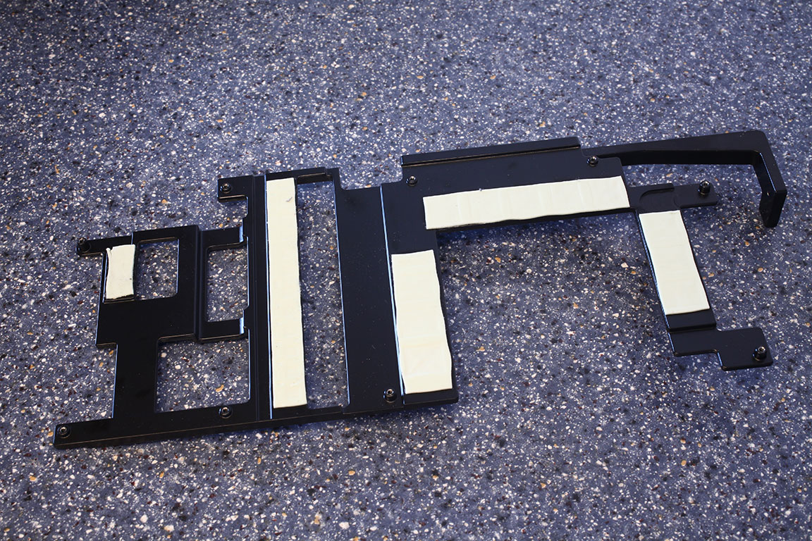
Under the heatsink/fan assembly a large metal heatspreader is located which cools memory chips, voltage circuitry and other secondary components. This approach can be useful for extreme overclockers as you can focus on LN2 cooling the GPU only and don't have to worry about the rest of the card, or you can use it to provide extra heating to avoid memory and VRM from getting too cold.
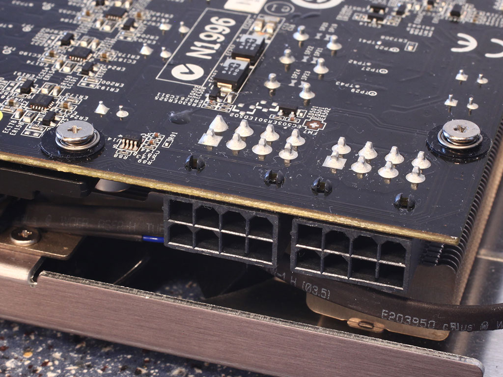
The card has two 8-pin PCI-Express power connectors which are specified up to 375 W power delivery - plenty of juice!
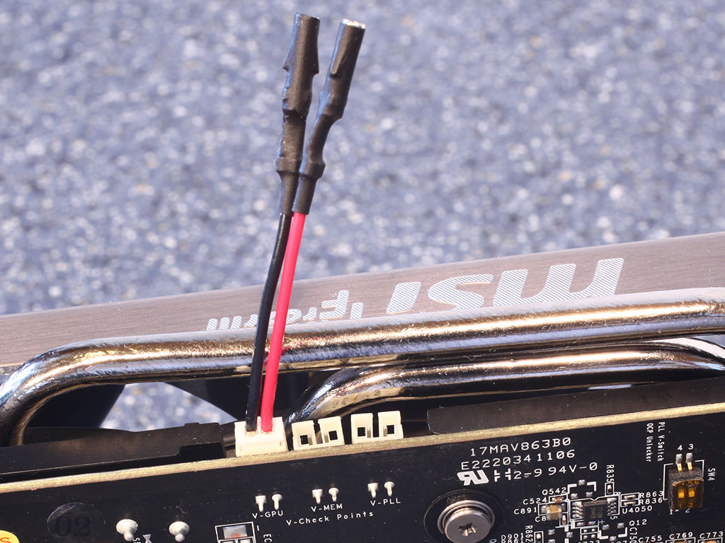
MSI has included three easy to access voltage measurement points near the top edge of the PCB. You have access to GPU Voltage, Memory Voltage and PLL Voltage. I attached one of the included measurement cables to the VGPU point to show how the system works - there are three cables included.
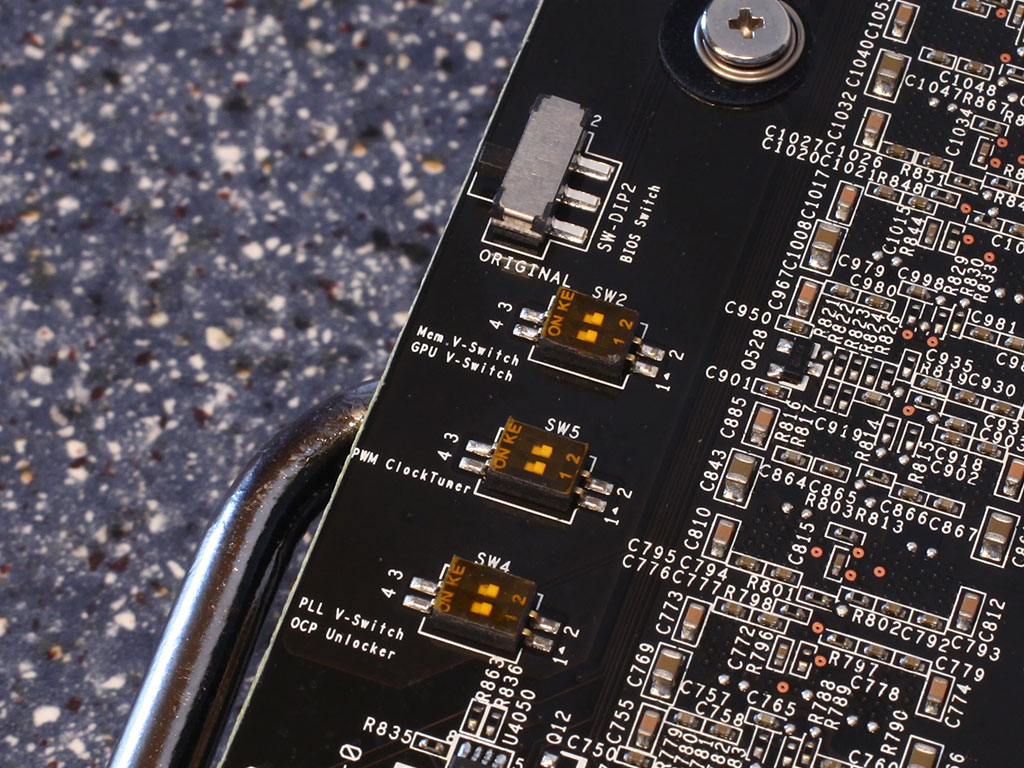
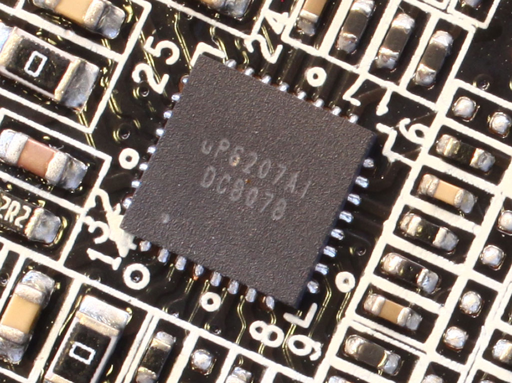
MSI has placed several DIP switches on the board for some basic non-software control of the card. Starting from the top you have Memory voltage and GPU voltage which provides an instant boost to those voltages, next we have PWM ClockTuner which lets you select the PWM clock frequency from 260 MHz to 310 MHz. Finally we have a switch to increase PLL voltage and one to remove the overcurrent protection of the card. An extra DIP switch is located near middle of the board and is used to enable several LN2 fixes which help with stability when using Liquid Nitrogen cooling.
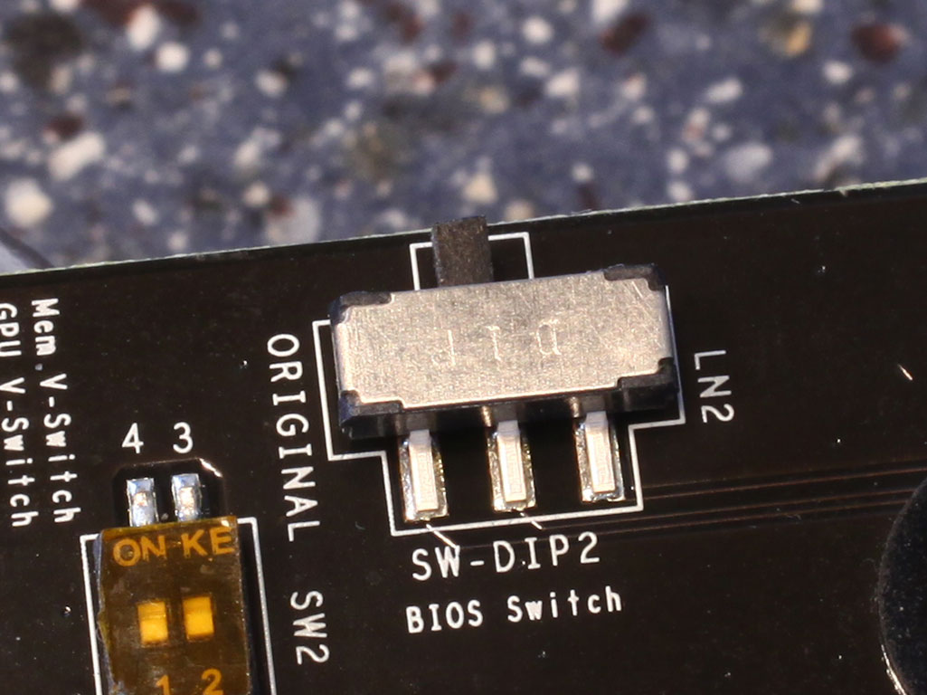
The BIOS switch will let you select between the default BIOS and a BIOS that has no cold slowdown issue. When GPU temperature goes negative, the GPU sometimes thinks it is overheating which would cause it to reduce clock speeds. Also the second BIOS serves as a backup in case something goes wrong during a BIOS flash.
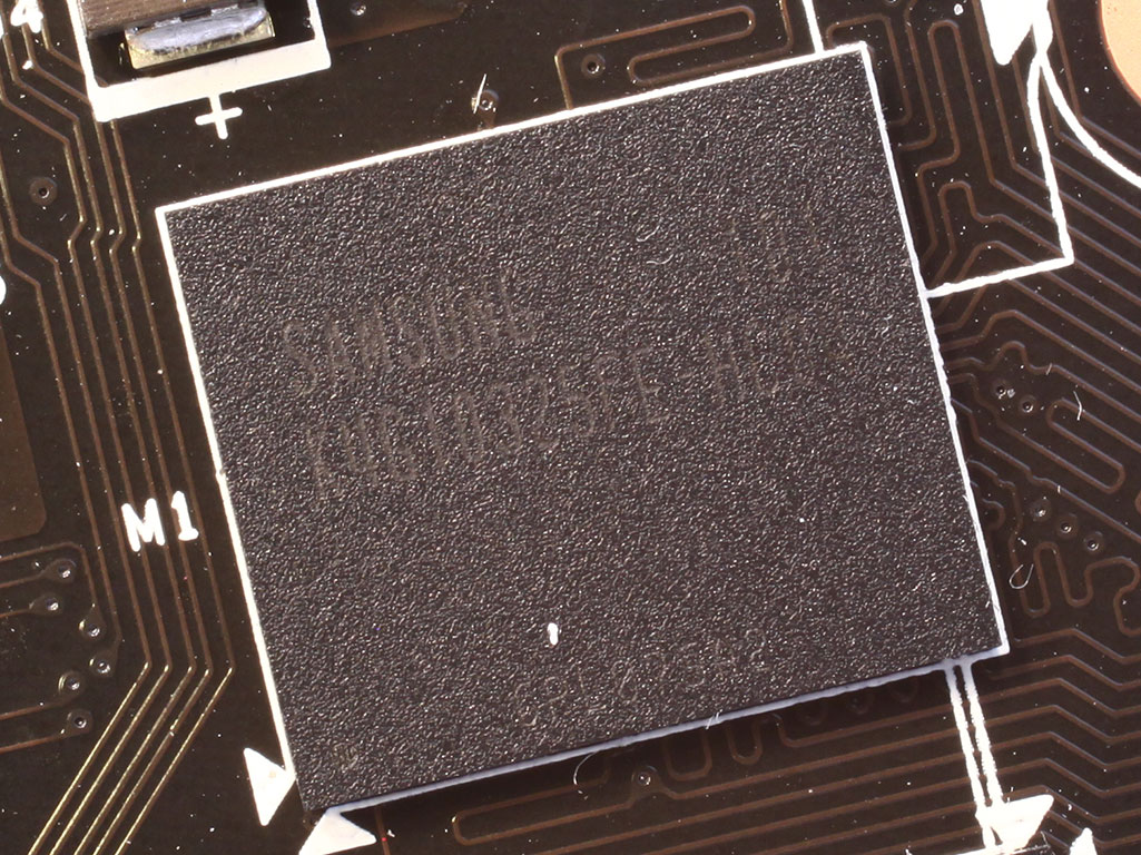
The GDDR5 memory chips are made by Samsung, and carry the model number K4G10325FE-HC04. They are specified to run at 1250 MHz (5000 MHz GDDR5 effective).
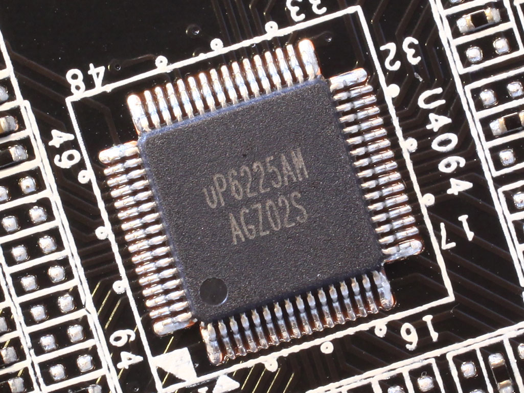
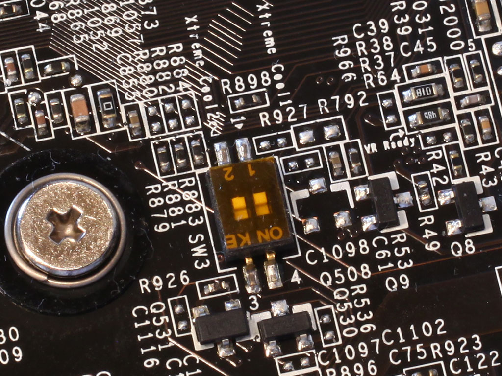
MSI has placed two voltage controllers on their card so several voltages can be controlled via software.
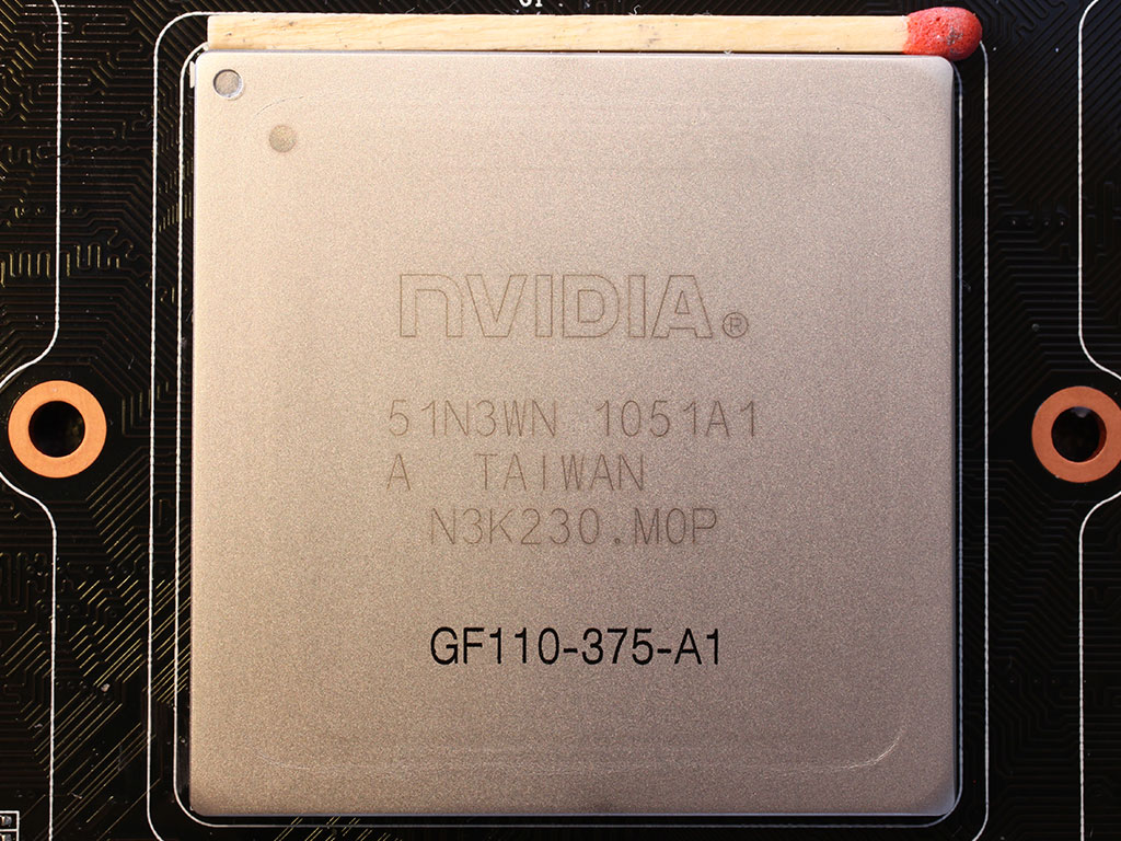
NVIDIA's GeForce 110 graphics processor is made on a 40 nm process at TSMC Taiwan. It uses approximately 3.0 billion transistors which is 200 million less than the GF100. Please note that the silvery metal surface you see is the heatspreader of the GPU. According to NVIDIA, the die size of the GF110 graphics processor is 520 mm².
Mar 6th, 2025 08:18 EST
change timezone
Latest GPU Drivers
New Forum Posts
- PS4 Cleaning but Rivets (3)
- Get 9070 or 9070 XT (45)
- Windows 11 General Discussion (5835)
- Flashing Rx7900xtx (1)
- intel 1700 with high speed ram,memory (18)
- Post your 7-Zip v22.01 scores (412)
- 6TB Iron Wolf $110 (7)
- TPU's Nostalgic Hardware Club (20059)
- GameTechBench GPU benchmark is already out! (302)
- Will I benefit from changing the thermal pad? (23)
Popular Reviews
- Sapphire Radeon RX 9070 XT Nitro+ Review - Beating NVIDIA
- NVIDIA GeForce RTX 5070 Founders Edition Review
- ASUS Radeon RX 9070 TUF OC Review
- AMD Radeon RX 9070 Series Technical Deep Dive
- EIZO FlexScan EV4340X Review - A Multitasking Powerhouse
- RAWM ES21M Review
- ASUS GeForce RTX 5070 Ti TUF OC Review
- AMD Ryzen 7 9800X3D Review - The Best Gaming Processor
- MSI GeForce RTX 5070 Ti Vanguard SOC Review
- MSI GeForce RTX 5070 Ti Ventus 3X OC Review
Controversial News Posts
- NVIDIA GeForce RTX 50 Cards Spotted with Missing ROPs, NVIDIA Confirms the Issue, Multiple Vendors Affected (513)
- AMD Plans Aggressive Price Competition with Radeon RX 9000 Series (277)
- AMD Radeon RX 9070 and 9070 XT Listed On Amazon - One Buyer Snags a Unit (261)
- AMD Mentions Sub-$700 Pricing for Radeon RX 9070 GPU Series, Looks Like NV Minus $50 Again (248)
- NVIDIA Investigates GeForce RTX 50 Series "Blackwell" Black Screen and BSOD Issues (244)
- AMD RDNA 4 and Radeon RX 9070 Series Unveiled: $549 & $599 (241)
- AMD Radeon RX 9070 and 9070 XT Official Performance Metrics Leaked, +42% 4K Performance Over Radeon RX 7900 GRE (195)
- AMD Radeon RX 9070-series Pricing Leaks Courtesy of MicroCenter (158)