 10
10
Neo Forza eSports NFP075 1 TB Review
(10 Comments) »Introduction
Neo Forza is a relatively young manufacturer of DRAM memory modules and flash memory products. The Taiwanese company was founded in 2018 as enthusiast-focused brand of Goldkey, a well-established producer of computer hardware which has focused on OEM manufacturing until recently.

Today's review covers the Neo Forza eSports M.2 NVMe SSD, which is also known as NFP075. "eSports" is not a range of products, but the name of this specific drive. A future Gen 4 drive would be called "Esports4x4", according to Neo Forza. Under the hood, the NFP075 is powered by a Phison PS5012-E12S controller paired with 3D TLC NAND from Chinese state-backed flash memory maker Yangtze Memory Technologies Co (YMTC)—the first YMTC flash I've ever reviewed! A DRAM chip from Kingston is included, too. PCI-Express 3.0 x4 is used as the host interface.
The Neo Forza eSports is available in capacities of 256 GB, 512 GB, 1 TB, and 2 TB. Endurance for these models is set at 420 TBW, 890 TBW, 1350 TBW, and 1550 TBW respectively. Neo Forza provides a three-year warranty for the eSports SSD.
| Specifications: Neo Forza eSports NFP075 1 TB | |
|---|---|
| Brand: | Neo Forza |
| Model: | NFP075PCI1T-3400200 |
| Capacity: | 1024 GB (953 GB usable) No additional overprovisioning |
| Controller: | Phison PS5012-E12S |
| Flash: | YMTC 64-Layer 3D TLC CABBG64A0A |
| DRAM: | 1x 256 MB Kingston DDR3-1866 D1216ECMDXGJD |
| Endurance: | 1350 TBW |
| Form Factor: | M.2 2280 |
| Interface: | PCIe Gen 3 x4, NVMe 1.3 |
| Device ID: | Neo Forza NFP075PCI1T-3400000 |
| Firmware: | ECFM32.1 |
| Warranty: | Three years |
| Price at Time of Review: | $130 / 13 cents per GB |
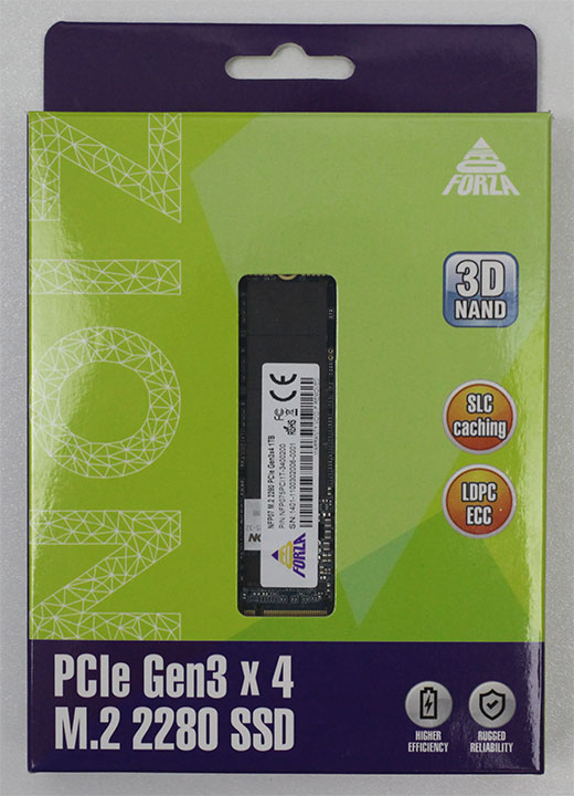
Packaging

The Drive

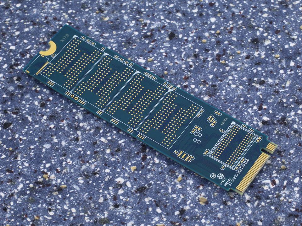
The drive uses the M.2 2280 form factor, which makes it 22 mm wide and 80 mm long.
Like most M.2 NVMe SSDs, the Neo Forza eSports connects to the host system over a PCI-Express 3.0 x4 interface.


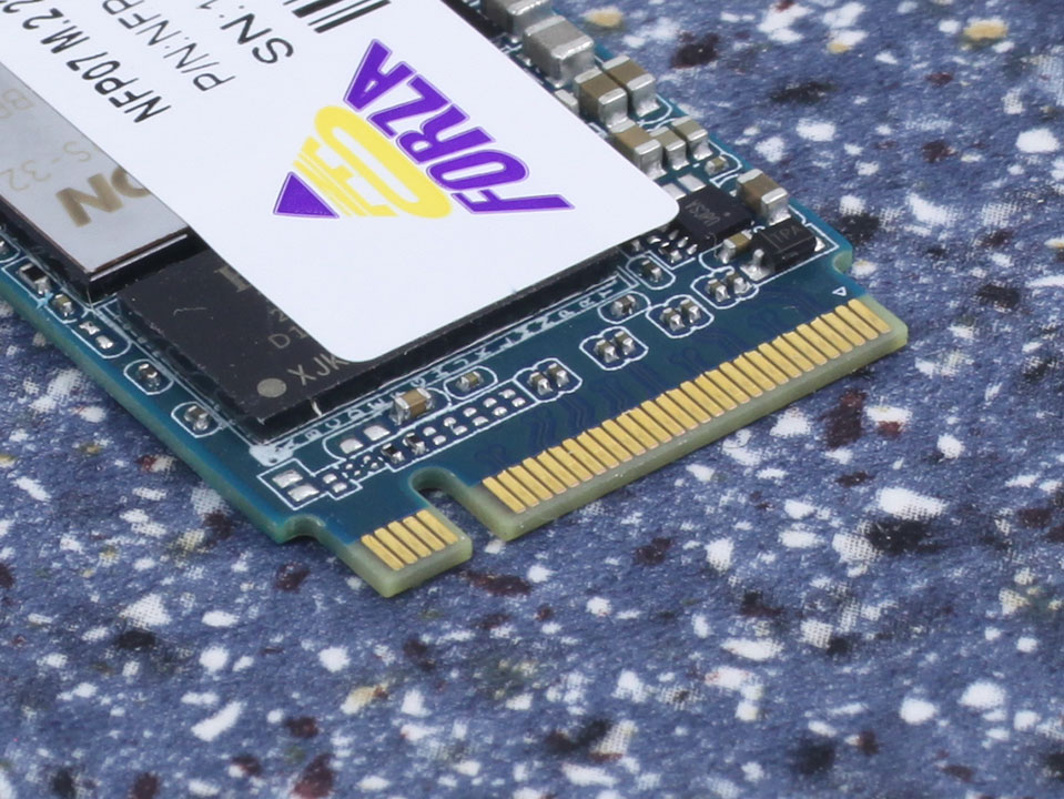
On the PCB, you'll find the controller, four flash chips, and one DRAM chip.
Chip Component Analysis
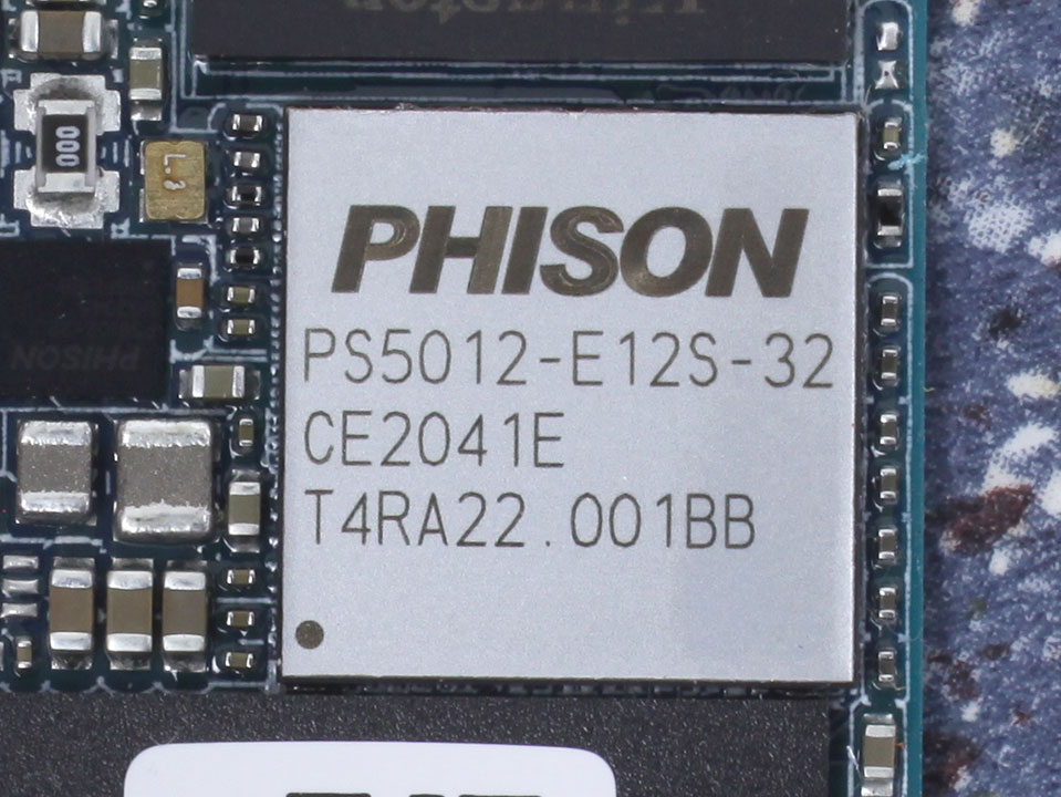
The flash controller is made by Phison and supports 3D TLC, QLC, and PCI-Express 3.0 x4. It uses eight flash channels and is produced on a 28 nm process at TSMC Taiwan.

The four 64-layer 3D TLC flash chips are made by YMTC, a Chinese NAND maker that is government-backed. YMTC has an exclusive 3D die-stacking technology called Xtacking, which enables them to claim the "3D TLC" title, more about the tech here. Basically, the NAND storage array is manufactured on a die separate to the CMOS control logic die. In manufacturing, both dies are stacked with vertical interconnections. Obviously this requires an extremely high degree of precision, but yields great density.
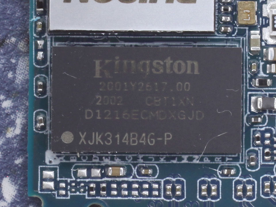
A single Kingston DDR3 chip provides 256 MB of DRAM storage for the controller to store the mapping tables. This is a surprisingly small amount of DRAM for a 1 TB SSD; normally, you'd expect 1 GB per 1 TB.
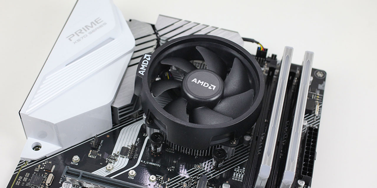
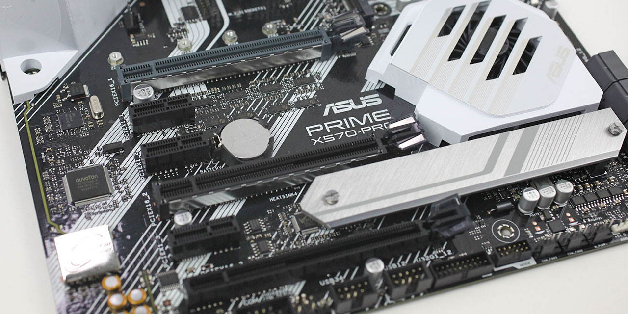
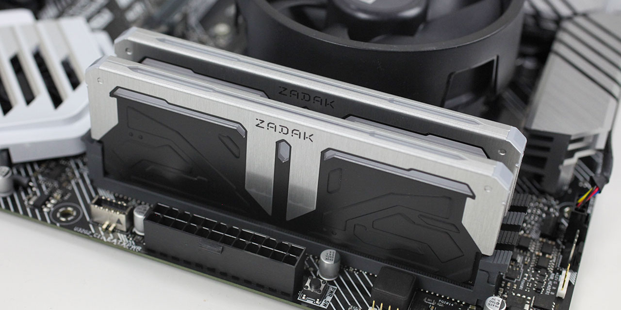
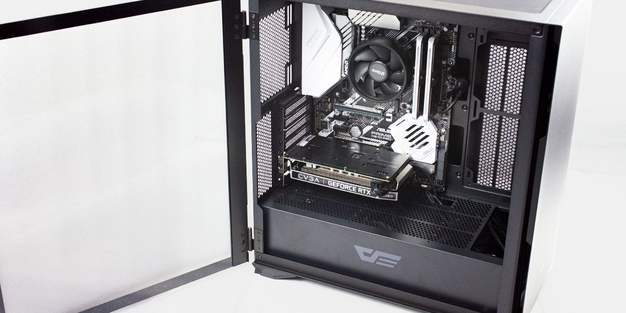
Test Setup
| Test System SSD 2021 | |
|---|---|
| Processor: | AMD Ryzen 3 3300X @ 4.3 GHz Zen 2, 16 MB Cache |
| Motherboard: | ASUS Prime X570-Pro BIOS 2606 / AGESA 1.0.8.0 |
| Memory: | Zadak Spark RGB, 16 GB DDR4 @ 3200 MHz 16-18-18-38 |
| Graphics: | EVGA GeForce RTX 2060 KO 6 GB |
| Case: | DarkFlash DLX22 |
| Operating System: | Windows 10 Professional 64-bit Version 2004 (May 2020 Update) |
| Drivers: | AMD Chipset: 2.07.14.327 NVIDIA: 452.06 WHQL |
Our Patreon Silver Supporters can read articles in single-page format.
Apr 9th, 2025 19:09 EDT
change timezone
Latest GPU Drivers
New Forum Posts
- What local LLM-s you use? (152)
- What is this temp sensor referring to? (0)
- Cache Ratio stuck at 600hz lower than Turbo Cores with Ring Down Bin on (3)
- Does anybody know a way to make a scratch on the glass case panel less noticeable or remove it? (21)
- Msi Vector 16HX Undervolt (10)
- Technical Issues - TPU Main Site & Forum (2025) (87)
- Asking before I mess up (1)
- What's your latest tech purchase? (23503)
- TPU's Nostalgic Hardware Club (20209)
- 9070XT or 7900XT or 7900XTX (178)
Popular Reviews
- The Last Of Us Part 2 Performance Benchmark Review - 30 GPUs Compared
- MCHOSE L7 Pro Review
- UPERFECT UStation Delta Max Review - Two Screens In One
- ASRock Z890 Taichi OCF Review
- Sapphire Radeon RX 9070 XT Pulse Review
- PowerColor Radeon RX 9070 Hellhound Review
- Upcoming Hardware Launches 2025 (Updated Apr 2025)
- Sapphire Radeon RX 9070 XT Nitro+ Review - Beating NVIDIA
- ASUS Prime X870-P Wi-Fi Review
- Acer Predator GM9000 2 TB Review
Controversial News Posts
- NVIDIA GeForce RTX 5060 Ti 16 GB SKU Likely Launching at $499, According to Supply Chain Leak (172)
- MSI Doesn't Plan Radeon RX 9000 Series GPUs, Skips AMD RDNA 4 Generation Entirely (146)
- Microsoft Introduces Copilot for Gaming (124)
- AMD Radeon RX 9070 XT Reportedly Outperforms RTX 5080 Through Undervolting (119)
- NVIDIA Reportedly Prepares GeForce RTX 5060 and RTX 5060 Ti Unveil Tomorrow (115)
- Over 200,000 Sold Radeon RX 9070 and RX 9070 XT GPUs? AMD Says No Number was Given (100)
- Nintendo Confirms That Switch 2 Joy-Cons Will Not Utilize Hall Effect Stick Technology (99)
- Nintendo Switch 2 Launches June 5 at $449.99 with New Hardware and Games (98)