 228
228
NVIDIA GeForce RTX 4080 Super Founders Edition Review - Savings of $200
Test Setup »High-resolution PCB Pictures
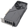
These pictures are for the convenience of volt modders and people who would like to see all the finer details on the PCB. Feel free to link back to us and use these in your articles, videos or forum posts.High-resolution versions are also available (front, back).
Circuit Board (PCB) Analysis
GPU voltage is an eleven-phase design, managed by a Monolithic Power Systems MP2891 controller, which also handles memory voltage.
Monolithic MP86957 DrMOS components are used for GPU voltage; they are rated for 70 A of current each.
Memory voltage is a two-phase design, managed by the same MP2891 that's used for GPU voltage.
For memory, Monolithic MP86957 DrMOS with a 70 A rating are used, too.
The GDDR6X memory chips are made by Micron and carry the model number D8BZF, which decodes to MT61K512M32KPA-24. They are specified to run at 1500 MHz (24 Gbps effective).
NVIDIA's AD103 graphics processor is the company's second Ada Lovelace GPU. It is built using a 5 nanometer process at TSMC Taiwan, with a transistor count of 45.9 billion and a die size of 379 mm².
Feb 21st, 2025 19:05 EST
change timezone
Latest GPU Drivers
New Forum Posts
- As we live the age of game remakes, which game you would like to see to have a remake? (309)
- [Intel AX1xx/AX2xx/AX4xx/AX16xx/BE2xx/BE17xx] Intel Modded Wi-Fi Driver with Intel® Killer™ Features (271)
- Nvidia's GPU market share hits 90% in Q4 2024 (gets closer to full monopoly) (420)
- Share your AIDA 64 cache and memory benchmark here (3012)
- [PCGamer] Former Sony exec finally says the quiet part out loud: putting PlayStation games on PC is 'almost like printing money' (39)
- A Final Fantasy IX Reminiscence - My love letter and homage to one of the best stories ever told (54)
- TPU's Nostalgic Hardware Club (19976)
- Should I make a thermal maintenance on my GPU? (72)
- 1st New Build! Any thoughts/feedback? (16)
- [Feature request] NIS and rBAR (11)
Popular Reviews
- MSI GeForce RTX 5070 Ti Ventus 3X OC Review
- Gigabyte GeForce RTX 5090 Gaming OC Review
- Galax GeForce RTX 5070 Ti 1-Click OC White Review
- ASUS GeForce RTX 5070 Ti TUF OC Review
- Ducky One X Inductive Keyboard Review
- MSI GeForce RTX 5070 Ti Vanguard SOC Review
- MSI GeForce RTX 5070 Ti Gaming Trio OC+ Review
- AMD Ryzen 7 9800X3D Review - The Best Gaming Processor
- MSI MAG Z890 Tomahawk Wi-Fi Review
- NVIDIA GeForce RTX 5080 Founders Edition Review
Controversial News Posts
- AMD Radeon 9070 XT Rumored to Outpace RTX 5070 Ti by Almost 15% (302)
- AMD Plans Aggressive Price Competition with Radeon RX 9000 Series (268)
- AMD is Taking Time with Radeon RX 9000 to Optimize Software and FSR 4 (256)
- AMD Radeon RX 9070 and 9070 XT Listed On Amazon - One Buyer Snags a Unit (247)
- NVIDIA GeForce RTX 5090 Spotted with Missing ROPs, Performance Loss Confirmed, Multiple Vendors Affected (241)
- Edward Snowden Lashes Out at NVIDIA Over GeForce RTX 50 Pricing And Value (241)
- AMD Denies Radeon RX 9070 XT $899 USD Starting Price Point Rumors (239)
- New Leak Reveals NVIDIA RTX 5080 Is Slower Than RTX 4090 (215)


