 140
140
NVIDIA GeForce GF100 Architecture Review
Geometry Processing & Tessellation »The NVIDIA GF100 GPU
NVIDIA's first consumer graphics implementation of its Fermi architecture is the GF100 graphics processor (GPU). Based on this, NVIDIA along with its partners may release one or two graphics card SKUs. A dual-GPU graphics board cannot be written off, either but is certainly not expected for launch. The GF100 is expected to be a ≥100% leap over the previous-generation GT200, in terms of raw compute power, transistor count, and the quantity and capability of various components within the GPU. It will be manufactured on TSMC's 40 nanometer silicon fabrication node.The GPU has the following physical specifications compared to existing GPU architectures from the present and previous generations:
| AMD Cypress | AMD RV790 | NVIDIA G92 | NVIDIA GT200 | NVIDIA GF100 | |
| Shader units | 1600 | 800 | 128 | 240 | 512 |
| ROPs | 32 | 16 | 16 | 32 | 48 |
| Texture Units | 80 | 40 | 64 | 80 | 64 |
| DirectX | 11 | 10.1 | 10 | 10 | 11 |
| Transistors | 2154M | 959M | 754M | 1400M | 3200M |
| Memory Type | GDDR5 | GDDR5 | GDDR3 | GDDR3 | GDDR5 |
| Memory Bus Width | 256 bit | 256 bit | 256 bit | 512 bit | 384 bit |
As you can see, NVIDIA gave the GF100 numerically a 115% increase in shader processors (now called "CUDA Cores" due to the versatility they have achieved beyond shading), a 50% increase in memory bandwidth compared to the GT200 (keeping memory clock speeds constant).

The GPU is organized in a manner described in the block diagram above. The Gigathread Engine acts as a complex crossbar that distributes workload between the highly parallel GPU components. A 384-bit GDDR5 memory controller connects the GPU to 12 memory chips, with an estimated 1536 MB (1.5 GB) or 3072 MB (3.0 GB) of memory, depending on the density of the memory chips used. It is also expected that we will see lower-end configurations with reduced number of memory chips, for example resulting in 256-bit cards with 1 GB of VRAM or 320 bit / 1280 MB. The processing complex of the GPU is arranged into four Graphics Processing Clusters, or GPCs (helps in modularity, combines four Streaming Multiprocessors or SMs to a raster engine), each GPC has a raster engine and four SMs (a sub-unit, combines 32 CUDA cores to common instruction and L1 caches, and a Polymorph Engine), each SM further has four texture mapping units (TMUs).
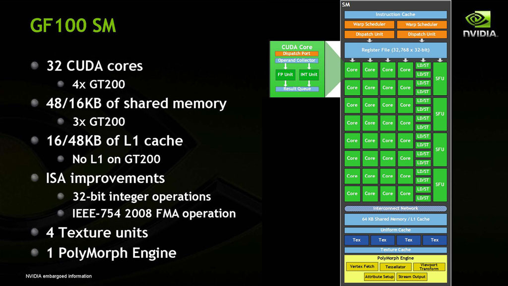
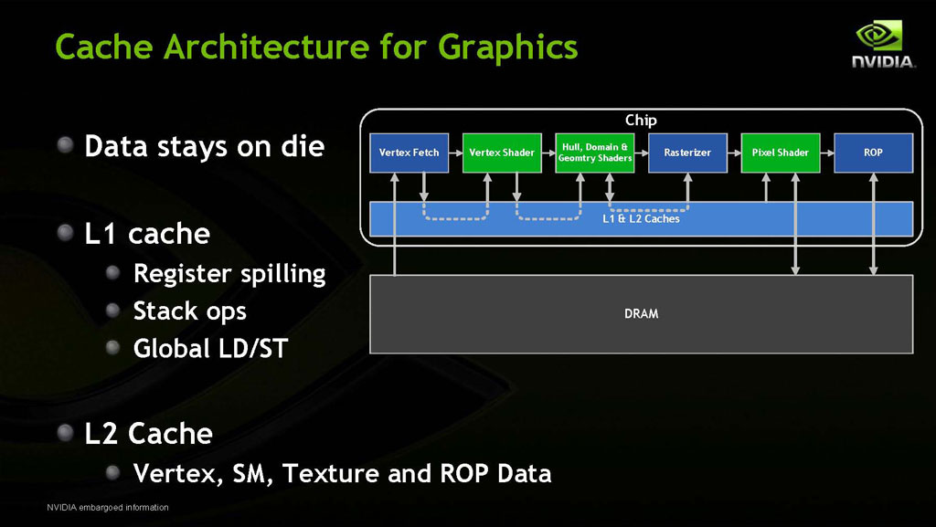
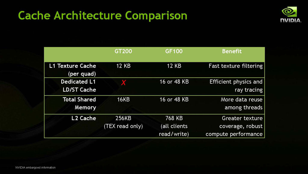
The level of parallelism is supported by caches at every level, which help manage data traffic, and let key instructions and data stay on the chip. There are shared 64 KB L1 caches on every SM, and a large 768 KB L2 cache for vertex, texture, and ROP data, among other general purpose functions. The 64 KB of L1 cache can be configured to be either 48 KB of shared memory and 16 KB of L1 cache or 48 KB of L1 cache with 16 KB shared memory - depending on the application.
Unlike competing GPUs with unified tessellators, NVIDIA's approach to tessellation involves distributing it among the 16 SMs using PolyMorph Engines. Each PolyMorph Engine gives the SM its own tessellator. Every GPC has its own Raster Engine. This hierarchy gives the GF100 a theoretical 8-times increase in geometry performance compared to the GT200, by decentralizing these components with a parallel architecture.

Mar 10th, 2025 13:32 EDT
change timezone
Latest GPU Drivers
New Forum Posts
- RX 9070 availability (166)
- MorePowerTool for RDNA 4. (0)
- AMD RX 9070 XT & RX 9070 non-XT thread (OC, undervolt, benchmarks, ...) (2)
- newegg ATX 3.1 PSU on Clearance and Free Fan (3)
- Nvidia's GPU market share hits 90% in Q4 2024 (gets closer to full monopoly) (770)
- AAF Optimus Modded Driver For Windows 10 & Windows 11 - Only for Realtek HDAUDIO Chips (375)
- DTS DCH Driver for Realtek HDA [DTS:X APO4 + DTS Interactive] (2110)
- Zen6 is almost here ? (45)
- Gaming PC instabiliity (16)
- It's happening again, melting 12v high pwr connectors (1019)
Popular Reviews
- Sapphire Radeon RX 9070 XT Nitro+ Review - Beating NVIDIA
- XFX Radeon RX 9070 XT Mercury OC Magnetic Air Review
- ASUS Radeon RX 9070 TUF OC Review
- MSI MAG B850 Tomahawk Max Wi-Fi Review
- NVIDIA GeForce RTX 5080 Founders Edition Review
- NVIDIA GeForce RTX 5070 Founders Edition Review
- Corsair Vengeance RGB CUDIMM DDR5-8800 48 GB CL42 Review
- AMD Ryzen 7 9800X3D Review - The Best Gaming Processor
- ASUS GeForce RTX 5070 Ti TUF OC Review
- MSI GeForce RTX 5070 Ti Gaming Trio OC+ Review
Controversial News Posts
- NVIDIA GeForce RTX 50 Cards Spotted with Missing ROPs, NVIDIA Confirms the Issue, Multiple Vendors Affected (513)
- AMD Plans Aggressive Price Competition with Radeon RX 9000 Series (277)
- AMD Radeon RX 9070 and 9070 XT Listed On Amazon - One Buyer Snags a Unit (261)
- AMD RDNA 4 and Radeon RX 9070 Series Unveiled: $549 & $599 (260)
- AMD Mentions Sub-$700 Pricing for Radeon RX 9070 GPU Series, Looks Like NV Minus $50 Again (248)
- NVIDIA Investigates GeForce RTX 50 Series "Blackwell" Black Screen and BSOD Issues (244)
- AMD Radeon RX 9070 and 9070 XT Official Performance Metrics Leaked, +42% 4K Performance Over Radeon RX 7900 GRE (195)
- AMD Radeon RX 9070-series Pricing Leaks Courtesy of MicroCenter (158)