 140
140
NVIDIA GeForce GF100 Architecture Review
(140 Comments) »Introduction
PC graphics got an overhaul with the new DirectX 11 API being released by Microsoft, along with its brand new Windows 7 operating system. A new generation of DirectX usually brings two things: 1st: GPUs with new features that piggy-back onto the new DirectX version's launch, and 2nd: GPUs that are significantly faster, while holding onto essentially the same market price-points. DirectX 11 is no exception.This time, AMD got to do the honors with its Radeon HD 5000 series GPUs, which has already become a generation of GPUs targeting nearly all price-points. NVIDIA, on the other hand invested time in developing a GPU in a way that has always worked for them: to make a powerful high-end monolithic GPU which dominates the upper quadrant, and then release derivatives based on it a little later. NVIDIA admitted to several developmental delays, due to 'unforeseen obstacles' for its GPU.
NVIDIA's new architecture codenamed "Fermi" was unveiled as early as on October 1st, 2009. Back then the move served as a market strategy more than anything, in the wake of AMD's launch of its DirectX 11 compliant Radeon HD 5800 series consumer graphics cards. It did however disclose a lot about the architecture NVIDIA was using, purely from the perspective of GPU computing, not touching anything on the subject of consumer graphics, DirectX 11 compliance, with game performance projections being a far cry. On hindsight, starting Fermi's press exposure from GPU computing was a wise move. It allowed NVIDIA to maintain ambiguity over the actual product's performance (in games, and in the market), while letting it talk about new technologies and features which would then allow the press to draw its inference from the press meet, and possibly chalk out its expectations from the consumer part.
It is that consumer part (implementation of the Fermi architecture in a consumer-grade GPU), which has taken shape deep within NVIDIA's caverns today, that the company is willing to share a lot more with the press about the architecture from a 'consumer graphics' standpoint, which also opens up some direct performance projections from the company. The new GPU is internally called "GF100" or "GeForce Fermi 100", we will put it under the looking glass, thanks to a recent NVIDIA presentation at CES.

The NVIDIA GF100 GPU
NVIDIA's first consumer graphics implementation of its Fermi architecture is the GF100 graphics processor (GPU). Based on this, NVIDIA along with its partners may release one or two graphics card SKUs. A dual-GPU graphics board cannot be written off, either but is certainly not expected for launch. The GF100 is expected to be a ≥100% leap over the previous-generation GT200, in terms of raw compute power, transistor count, and the quantity and capability of various components within the GPU. It will be manufactured on TSMC's 40 nanometer silicon fabrication node.The GPU has the following physical specifications compared to existing GPU architectures from the present and previous generations:
| AMD Cypress | AMD RV790 | NVIDIA G92 | NVIDIA GT200 | NVIDIA GF100 | |
| Shader units | 1600 | 800 | 128 | 240 | 512 |
| ROPs | 32 | 16 | 16 | 32 | 48 |
| Texture Units | 80 | 40 | 64 | 80 | 64 |
| DirectX | 11 | 10.1 | 10 | 10 | 11 |
| Transistors | 2154M | 959M | 754M | 1400M | 3200M |
| Memory Type | GDDR5 | GDDR5 | GDDR3 | GDDR3 | GDDR5 |
| Memory Bus Width | 256 bit | 256 bit | 256 bit | 512 bit | 384 bit |
As you can see, NVIDIA gave the GF100 numerically a 115% increase in shader processors (now called "CUDA Cores" due to the versatility they have achieved beyond shading), a 50% increase in memory bandwidth compared to the GT200 (keeping memory clock speeds constant).

The GPU is organized in a manner described in the block diagram above. The Gigathread Engine acts as a complex crossbar that distributes workload between the highly parallel GPU components. A 384-bit GDDR5 memory controller connects the GPU to 12 memory chips, with an estimated 1536 MB (1.5 GB) or 3072 MB (3.0 GB) of memory, depending on the density of the memory chips used. It is also expected that we will see lower-end configurations with reduced number of memory chips, for example resulting in 256-bit cards with 1 GB of VRAM or 320 bit / 1280 MB. The processing complex of the GPU is arranged into four Graphics Processing Clusters, or GPCs (helps in modularity, combines four Streaming Multiprocessors or SMs to a raster engine), each GPC has a raster engine and four SMs (a sub-unit, combines 32 CUDA cores to common instruction and L1 caches, and a Polymorph Engine), each SM further has four texture mapping units (TMUs).
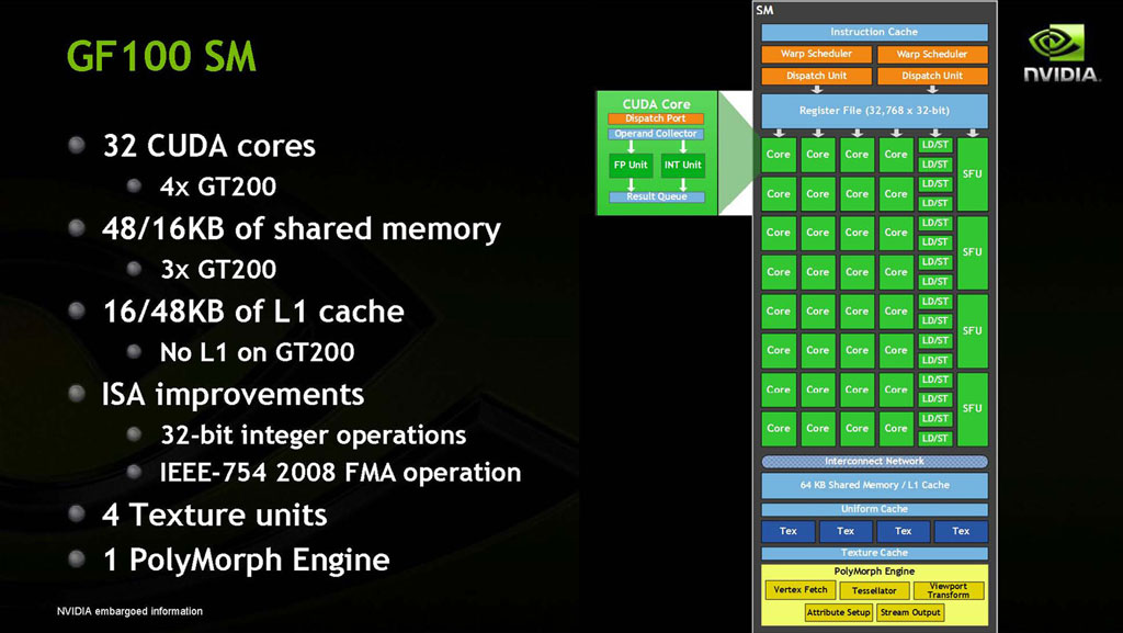
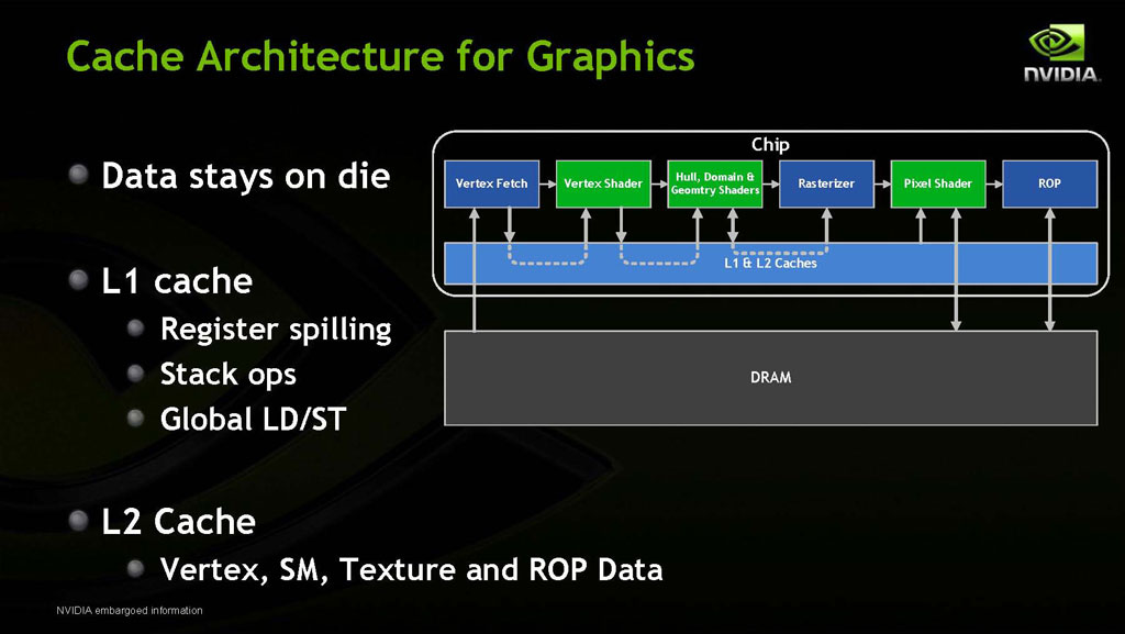
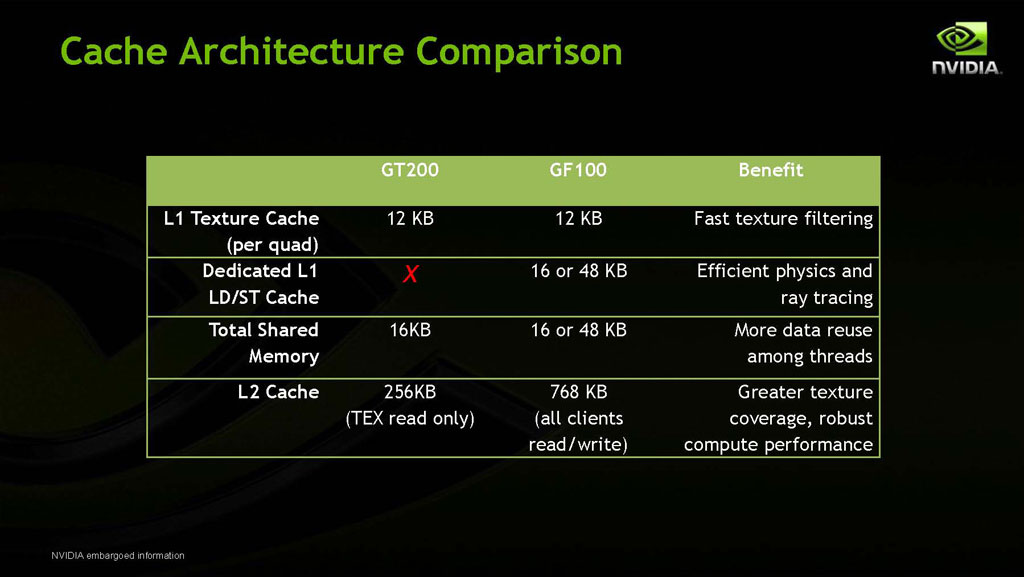
The level of parallelism is supported by caches at every level, which help manage data traffic, and let key instructions and data stay on the chip. There are shared 64 KB L1 caches on every SM, and a large 768 KB L2 cache for vertex, texture, and ROP data, among other general purpose functions. The 64 KB of L1 cache can be configured to be either 48 KB of shared memory and 16 KB of L1 cache or 48 KB of L1 cache with 16 KB shared memory - depending on the application.
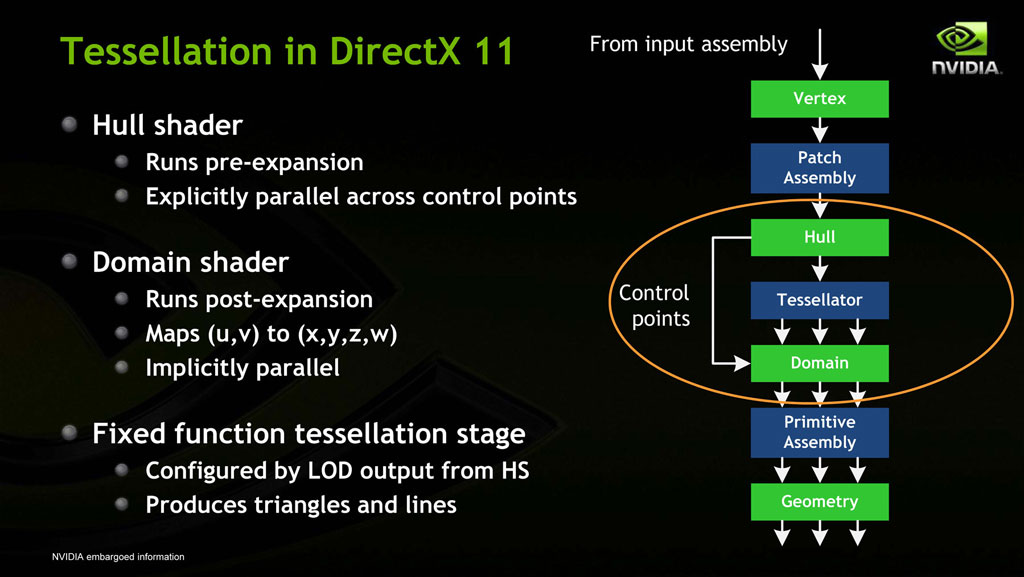
Unlike competing GPUs with unified tessellators, NVIDIA's approach to tessellation involves distributing it among the 16 SMs using PolyMorph Engines. Each PolyMorph Engine gives the SM its own tessellator. Every GPC has its own Raster Engine. This hierarchy gives the GF100 a theoretical 8-times increase in geometry performance compared to the GT200, by decentralizing these components with a parallel architecture.

Geometry Processing & Tessellation
One of the slides makes a very important observation that over the past five generations of GeForce GPUs since the GeForce FX 5800, geometry processing ability of GPUs, and the geometric complexity of games have seen stunted development when compared to shader performance and implementation. While the performance and complexity of the shader domain grew by over 150 times between these generations, that of geometry pretty much took the back seat with less than 3 times increment in geometry performance. This is what has come in the way of games being as photo-realistic as movies with 3D graphics, where the producers splurge on rendering farms that take care of high geometric complexity.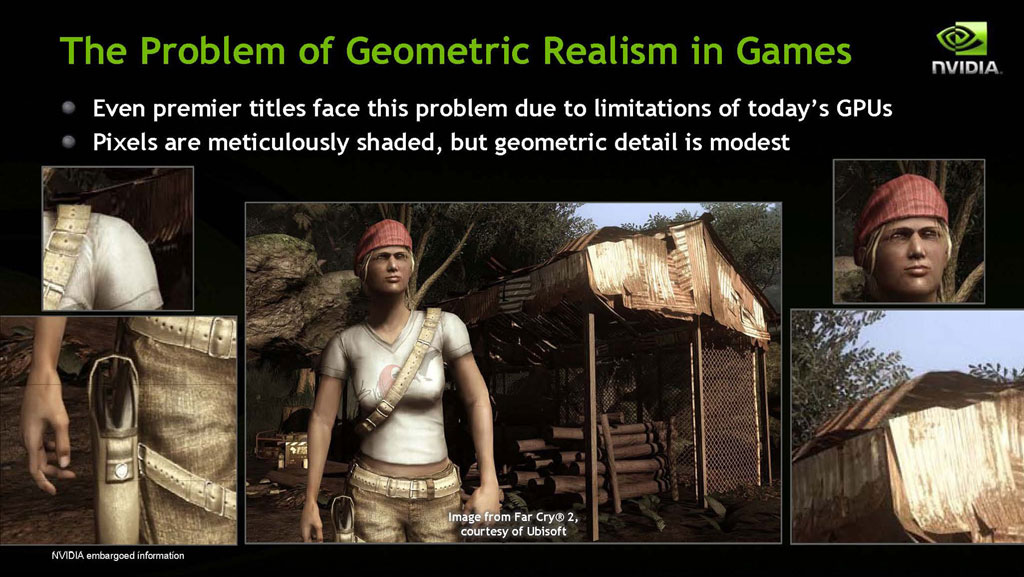
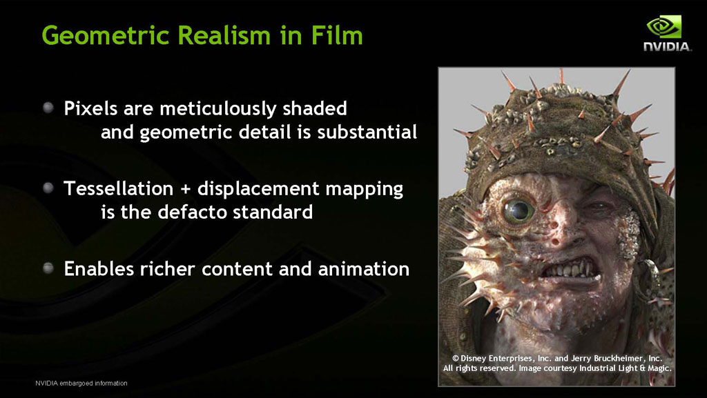
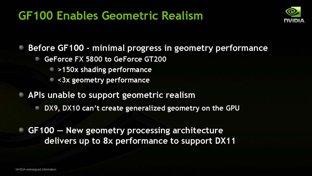
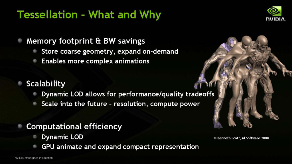
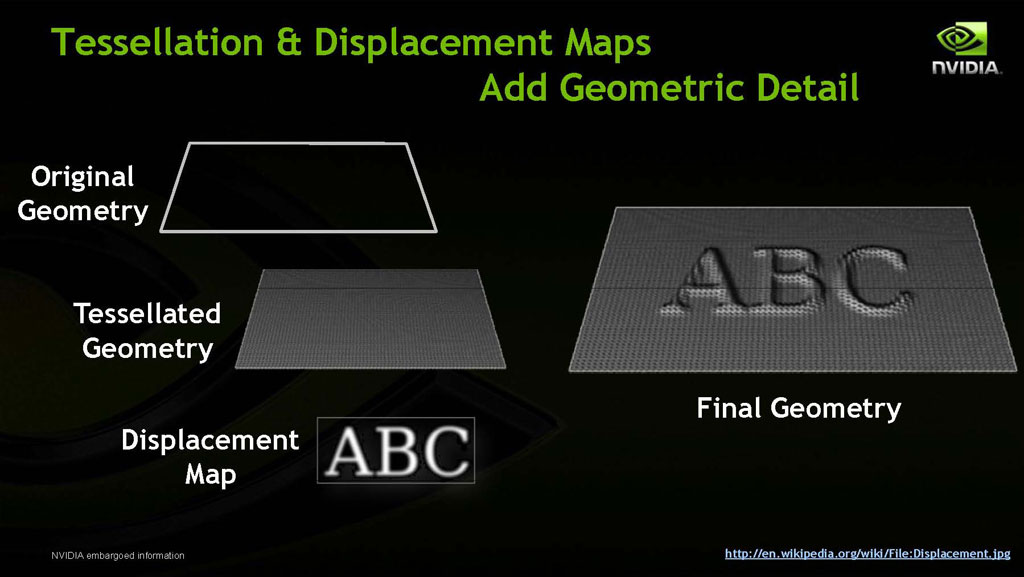
Tesselation is the way forward for geometric complexity to keep up with today's 3D graphics. The more complex the geometry of a 3D object is, the more accurately its shape is drawn on the screen. Tessellation allows the GPU to focus its resources on select portions of the 3D object where more complexity is required as instructed by a displacement map, and add to its geometric detail. DirectX 11 allows the GPU to create generalized geometry.
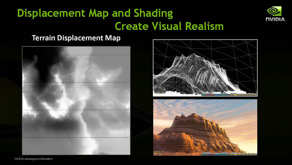
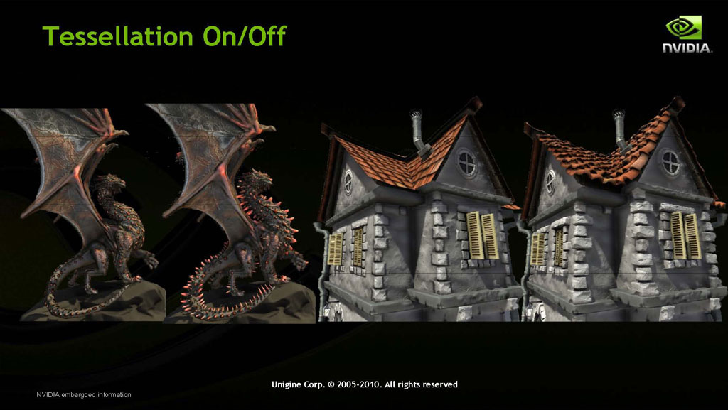
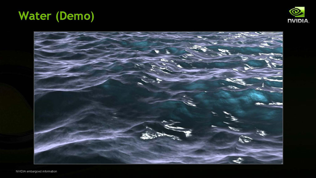
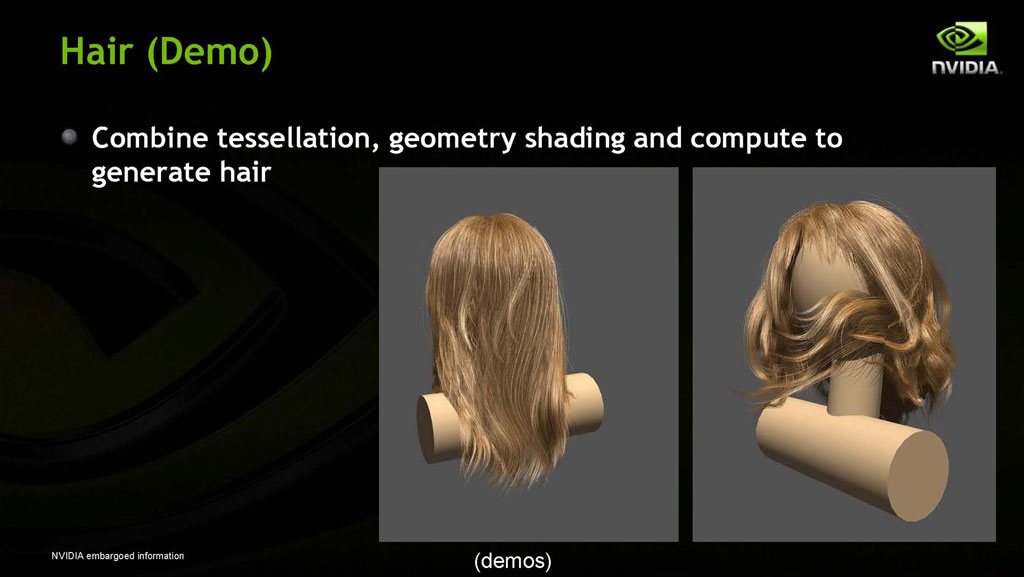
The following slides describe the way tessellation works in DirectX 11, and a few demos.
Our Patreon Silver Supporters can read articles in single-page format.
Mar 30th, 2025 03:15 EDT
change timezone
Latest GPU Drivers
New Forum Posts
- Can you guess Which game it is? (19)
- Did Nvidia purposely gimp the performance of 50xx series cards with drivers (126)
- RTX 5090 very slow while rendering or video/photo editing. (8)
- What are you playing? (23313)
- Windows 10 Vs 11, Which one too choose? (124)
- 13500 or 14500 or 12700 or 12700k (0)
- GPU Crashing System From Hibernation (10)
- Upgrade from a AMD AM3+ to AM4 or AM5 chipset MB running W10? (61)
- PCI 4.0 16x slot reported as a PCI 5.0 8x with the AMD 9070 XT Reaper GPU (39)
- The TPU UK Clubhouse (26006)
Popular Reviews
- Sapphire Radeon RX 9070 XT Pulse Review
- ASRock Phantom Gaming B850 Riptide Wi-Fi Review - Amazing Price/Performance
- Samsung 9100 Pro 2 TB Review - The Best Gen 5 SSD
- Palit GeForce RTX 5070 GamingPro OC Review
- Assassin's Creed Shadows Performance Benchmark Review - 30 GPUs Compared
- Sapphire Radeon RX 9070 XT Nitro+ Review - Beating NVIDIA
- ASRock Radeon RX 9070 XT Taichi OC Review - Excellent Cooling
- Enermax REVOLUTION D.F. 12 850 W Review
- AMD Ryzen 7 9800X3D Review - The Best Gaming Processor
- AMD Ryzen 9 9950X3D Review - Great for Gaming and Productivity
Controversial News Posts
- AMD RDNA 4 and Radeon RX 9070 Series Unveiled: $549 & $599 (260)
- MSI Doesn't Plan Radeon RX 9000 Series GPUs, Skips AMD RDNA 4 Generation Entirely (142)
- Microsoft Introduces Copilot for Gaming (124)
- AMD Radeon RX 9070 XT Reportedly Outperforms RTX 5080 Through Undervolting (119)
- NVIDIA Reportedly Prepares GeForce RTX 5060 and RTX 5060 Ti Unveil Tomorrow (115)
- Over 200,000 Sold Radeon RX 9070 and RX 9070 XT GPUs? AMD Says No Number was Given (100)
- NVIDIA GeForce RTX 5050, RTX 5060, and RTX 5060 Ti Specifications Leak (96)
- Retailers Anticipate Increased Radeon RX 9070 Series Prices, After Initial Shipments of "MSRP" Models (90)