 38
38
Sapphire HD 4890 1 GB GDDR5 Review
(38 Comments) »Introduction
Today AMD announced their Radeon HD 4890 Series. It is based on the RV790 GPU which is an improved version of the RV770. The major cornerstone specifications have remained the same, only improvements related to clock frequencies have been made. While it was almost impossible to get an RV770 to run far beyond 800 MHz, the ATI HD 4890 reference runs at 850 MHz core by default. Many partners will be offering overclocked boards as well ranging up to 1000 MHz core speed.
We have three HD 4890 reviews for you today:
Sapphire HD 4890 (this review), PowerColor HD 4890 and AMD HD 4890 CrossFire. While AMD has been sending out overclocked cards running at 900 MHz, our cards are based on the reference design clocks of 850 MHz.
| GeForce 9800 GT | Radeon HD 4850 | GeForce 9800 GTX | GeForce GTS 250 1 GB | GeForce GTX 260 | Radeon HD 4870 | Radeon HD 4890 | GeForce GTX 275 | GeForce GTX 280 | Radeon HD 4870 X2 | GeForce GTX 285 | |
| Shader units | 112 | 800 | 128 | 128 | 192 | 800 | 800 | 240 | 240 | 2x 800 | 240 |
| ROPs | 16 | 16 | 16 | 16 | 28 | 16 | 16 | 32 | 32 | 2x 16 | 32 |
| GPU | G92 | RV770 | G92 | G92 | GT200 | RV770 | RV790 | GT200 | GT200 | 2x RV770 | GT200b |
| Transistors | 754M | 956M | 754M | 754M | 1400M | 956M | 959M | 1400M | 1400M | 2x 956M | 1400M |
| Memory Size | 512 MB | 512 MB | 512 MB | 1024 MB | 896 MB | 512 MB | 1024 MB | 896 MB | 1024 MB | 2x 1024 MB | 1024 MB |
| Memory Bus Width | 256 bit | 256 bit | 256 bit | 256 bit | 448 bit | 256 bit | 256 bit | 448 bit | 512 bit | 2x 256 bit | 512 bit |
| Core Clock | 600 MHz | 625 MHz | 675 MHz | 738 MHz | 576 MHz | 750 MHz | 850 MHz | 633 MHz | 602 MHz | 750 MHz | 648 MHz |
| Memory Clock | 900 MHz | 993 MHz | 1100 MHz | 1100 MHz | 999 MHz | 900 MHz | 975 MHz | 1134 MHz | 1107 MHz | 900 MHz | 1242 MHz |
| Price | $110 | $140 | $160 | $149 | $240 | $190 | $249 | $249 | $315 | $425 | $350 |
Packaging & Contents

We received the card from Sapphire in an unprinted brown box. The picture above represents how the final package of the card will look like.

You will receive:
- Graphics card
- Documentation + Driver CD
- Cyberlink PowerDVD + Cyberlink PowerDirector + 3DMark Vantage Full Version
- CrossFire bridge
- PCI-Express power cables
- DVI Adapter + HDMI Adapter
- TV out Adapter + Cables
The Card


Sapphire uses the AMD reference design PCB and cooler with their own sticker on it. On the sample we reviewed, the final artwork is not present, so a picture was provided by Sapphire with the final design.

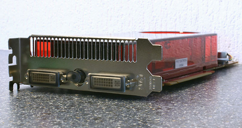
The card has two DVI ports, the most common output configuration today. If you want to use the card with your big TV screen you can use the included HDMI adapter. In case you need an analog port you can also use the included DVI adapter.
For HDMI Audio, NVIDIA requires you to feed an external audio source, for example from your motherboard's on-board audio, to the card via SPDIF cable. AMD on the other hand has integrated a sound device inside their GPUs which is the easier solution for most users.
The HD 4890 supports double, triple and quad CrossFire configurations for improved performance or better image quality.

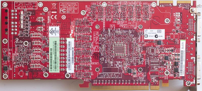
Here are the front and the back of the card, high-res versions are also available (front, back). If you choose to use these images for voltmods etc, please include a link back to this site or let us post your article.
A Closer Look


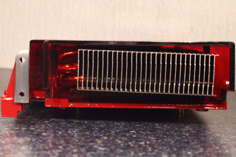
AMD's HD 4890 cooler is very similar to that of the HD 4870. It uses a copper base plate that is connected to a bigger heatsink via heatpipes. The fan design exhausts hot air outside of the case.
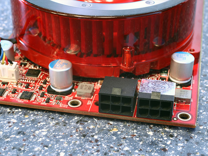
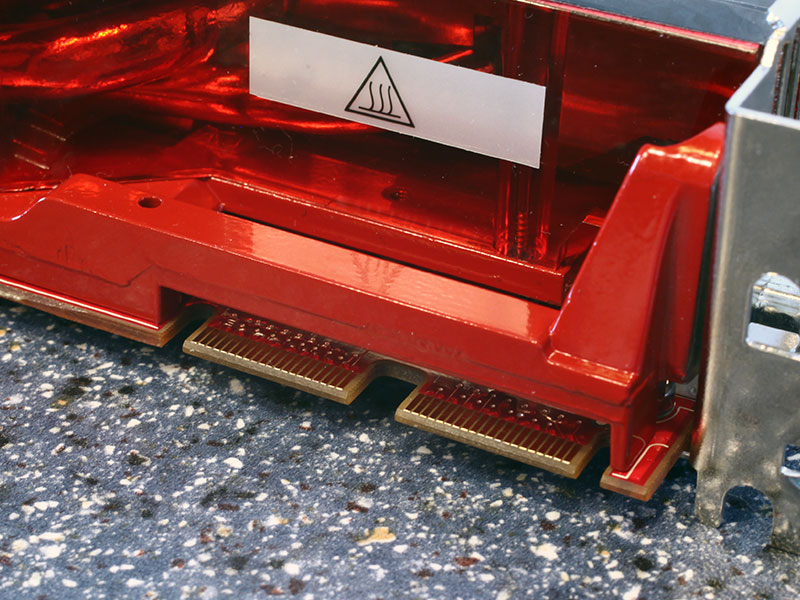
Two six pin power connectors are present on the reference design. Both are required for operation of the card.
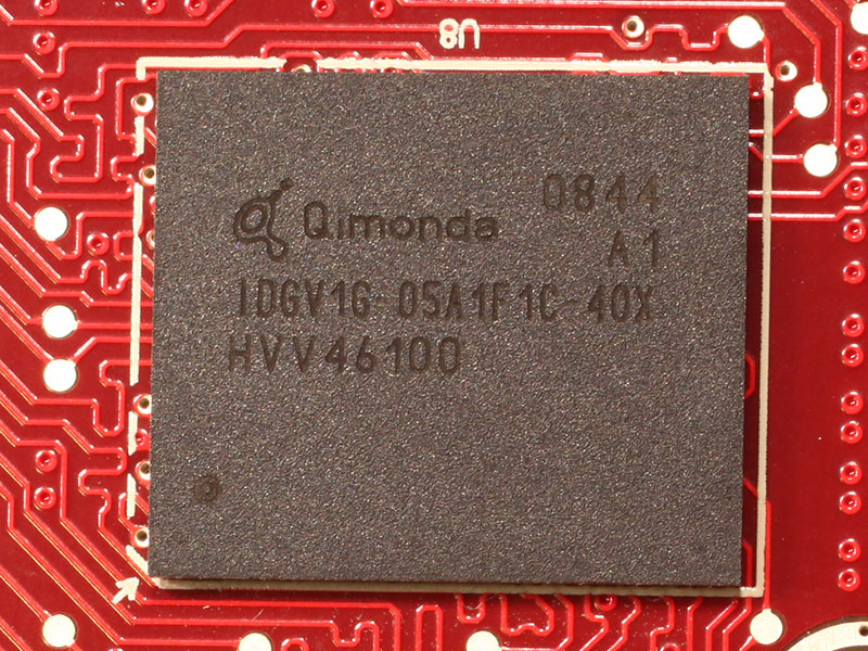
The GDDR5 memory chips are made by Qimonda and carry the model number IDGV1G-05A1F1C-40X. With a cycle time of 1.0 ns, they are specified to run at 1000 MHz.

AMD has put two VT1165 voltage controllers on their cards. One is responsible for the VGPU core voltage and the second one controls the memory voltage. This is very nice for overclockers because they can now change both voltages via software. For the average joe, it is a production cost increase that seems quite unnecessary.

This is AMD's new RV790 GPU. It is made in a 55 nm process at TSMC Taiwan with 959 million transistors. Please note that the die size is slightly increased from the RV770, the exact reason for that is unknown.
Our Patreon Silver Supporters can read articles in single-page format.
Apr 8th, 2025 16:33 EDT
change timezone
Latest GPU Drivers
New Forum Posts
- The Official Thermal Interface Material thread (1699)
- 9070XT or 7900XT or 7900XTX (151)
- Is RX 9070 VRAM temperature regular value or hotspot? (337)
- Show us your backside! (20)
- Kindly help in Identifying GPU and Suitable bios (15)
- ThrottleStop - 14900HX, 4090RTX MSI laptop (5)
- Entry level 4K gaming RIG for cRPG and h'n's games - Ryzen 5 5600 + RX 7600? (68)
- I have a bricked XFX Radeon RX 580 8GB GPU. HELP! (22)
- Have you got pie today? (16653)
- Milestones (14015)
Popular Reviews
- The Last Of Us Part 2 Performance Benchmark Review - 30 GPUs Compared
- UPERFECT UStation Delta Max Review - Two Screens In One
- MCHOSE L7 Pro Review
- PowerColor Radeon RX 9070 Hellhound Review
- Upcoming Hardware Launches 2025 (Updated Apr 2025)
- ASUS Prime X870-P Wi-Fi Review
- Sapphire Radeon RX 9070 XT Pulse Review
- Sapphire Radeon RX 9070 XT Nitro+ Review - Beating NVIDIA
- Corsair RM750x Shift 750 W Review
- DDR5 CUDIMM Explained & Benched - The New Memory Standard
Controversial News Posts
- NVIDIA GeForce RTX 5060 Ti 16 GB SKU Likely Launching at $499, According to Supply Chain Leak (162)
- MSI Doesn't Plan Radeon RX 9000 Series GPUs, Skips AMD RDNA 4 Generation Entirely (146)
- Microsoft Introduces Copilot for Gaming (124)
- AMD Radeon RX 9070 XT Reportedly Outperforms RTX 5080 Through Undervolting (119)
- NVIDIA Reportedly Prepares GeForce RTX 5060 and RTX 5060 Ti Unveil Tomorrow (115)
- Over 200,000 Sold Radeon RX 9070 and RX 9070 XT GPUs? AMD Says No Number was Given (100)
- Nintendo Switch 2 Launches June 5 at $449.99 with New Hardware and Games (97)
- NVIDIA GeForce RTX 5050, RTX 5060, and RTX 5060 Ti Specifications Leak (97)