 29
29
Sapphire Radeon RX 7700 XT Pulse Review
(29 Comments) »Introduction
Sapphire Radeon RX 7700 XT Pulse is the company's cost-effective custom-design rendition of AMD's swanky new performance segment graphics card being launched today. We are celebrating the double launch of the new RX 7700 XT and RX 7800 XT, be sure to check out our extensive coverage of 9 graphics card reviews on launch day. The Sapphire Pulse family of graphics cards is designed for those who want a Radeon RX graphics card that they can just install and forget about. There are no flashy product aesthetics or LED lighting, but you get a card that's compact, and which you can easily maintain over a long period of time.

The new Radeon RX 7700 XT is designed for maxed out 1440p gaming, just like the RX 7800 XT, but at a more attractive price-point, with prices starting at $450. You have all the muscle you need for AAA and e-sports gaming at 1440p, or high refresh-rate 1080p gaming. The RX 7700 XT is based on the latest RDNA 3 graphics architecture, which brings you generational performance improvements, new features such as AI acceleration and multi-draw indirect accelerator; and next-generation energy efficiency thanks to the new 5 nm foundry process where it matters.
The RX 7700 XT is carved out of the same Navi 32 chiplet GPU as the RX 7800 XT. Much like the Navi 31 GPU powering the RX 7900 series, the Navi 32 sees the GPU's main graphics rendering and number crunching machinery located on a centralized 5 nm die called the graphics compute die (GCD), surrounded by four dies that each contain a 16 MB segment of the GPU's Infinity Cache, and a 64-bit portion of the GPU's memory interface. The RX 7700 XT is configured with three out of four MCDs, which gives it 48 MB of Infinity Cache, and a 192-bit wide memory interface, which drives 12 GB of 18 Gbps GDDR6 memory, yielding 432 GB/s of memory bandwidth.
The 5 nm GCD of the RX 7700 XT is configured with 54 RDNA 3 compute units, which work out to 3,456 stream processors, 108 AI accelerators, 54 Ray accelerators, 216 TMUs, and 96 ROPs. AMD runs the GPU at 2171 MHz game clocks, and 2544 MHz boost. Internally, the GPU's front-end runs at 10-15% higher clocks than the shader engines. Sapphire has configured the RX 7700 XT Pulse with a power limit of 230 W.
The Sapphire RX 7700 XT Pulse features a simple aluminium fin-stack based cooling solution that's ventilated by a pair of axial flow fans. Sapphire designed the cooler such that you can disassemble the cooler shroud holding these fans without disturbing the heatsink underneath, so you can periodically clean the fans. Besides this, as we mentioned earlier, the design focus really is to give the gamer a quiet card that's easy to install. The card is easy on the pocket, too, priced at the AMD MSRP of $450.
Short 10-Minute Video Comparing 9x RX 7800 XT and RX 7700 XT
Our goal with the videos is to create short summaries, not go into all the details and test results, which can be found in our written reviews.
| Price | Cores | ROPs | Core Clock | Boost Clock | Memory Clock | GPU | Transistors | Memory | |
|---|---|---|---|---|---|---|---|---|---|
| RTX 3060 | $250 | 3584 | 48 | 1320 MHz | 1777 MHz | 1875 MHz | GA106 | 12000M | 12 GB, GDDR6, 192-bit |
| RX 7600 | $250 | 2048 | 64 | 2250 MHz | 2625 MHz | 2250 MHz | Navi 33 | 13300M | 8 GB, GDDR6, 128-bit |
| RTX 4060 | $290 | 3072 | 48 | 1830 MHz | 2460 MHz | 2125 MHz | AD107 | 18900M | 8 GB, GDDR6, 128-bit |
| Arc A770 | $250 | 4096 | 128 | 2100 MHz | N/A | 2187 MHz | ACM-G10 | 21700M | 16 GB, GDDR6, 256-bit |
| RTX 2080 | $240 | 2944 | 64 | 1515 MHz | 1710 MHz | 1750 MHz | TU104 | 13600M | 8 GB, GDDR6, 256-bit |
| RTX 3060 Ti | $260 | 4864 | 80 | 1410 MHz | 1665 MHz | 1750 MHz | GA104 | 17400M | 8 GB, GDDR6, 256-bit |
| RTX 4060 Ti | $390 | 4352 | 48 | 2310 MHz | 2535 MHz | 2250 MHz | AD106 | 22900M | 8 GB, GDDR6, 128-bit |
| RX 6700 XT | $310 | 2560 | 64 | 2424 MHz | 2581 MHz | 2000 MHz | Navi 22 | 17200M | 12 GB, GDDR6, 192-bit |
| RTX 2080 Ti | $350 | 4352 | 88 | 1350 MHz | 1545 MHz | 1750 MHz | TU102 | 18600M | 11 GB, GDDR6, 352-bit |
| RTX 3070 | $300 | 5888 | 96 | 1500 MHz | 1725 MHz | 1750 MHz | GA104 | 17400M | 8 GB, GDDR6, 256-bit |
| RTX 3070 Ti | $390 | 6144 | 96 | 1575 MHz | 1770 MHz | 1188 MHz | GA104 | 17400M | 8 GB, GDDR6X, 256-bit |
| RX 6800 | $430 | 3840 | 96 | 1815 MHz | 2105 MHz | 2000 MHz | Navi 21 | 26800M | 16 GB, GDDR6, 256-bit |
| RX 7700 XT | $450 | 3456 | 96 | 2171 MHz | 2544 MHz | 2250 MHz | Navi 32 | 26500M | 12 GB, GDDR6, 192-bit |
| Sapphire RX 7700 XT Pulse | $450 | 3456 | 96 | 2171 MHz | 2544 MHz | 2250 MHz | Navi 32 | 26500M | 12 GB, GDDR6, 192-bit |
| RX 6800 XT | $510 | 4608 | 128 | 2015 MHz | 2250 MHz | 2000 MHz | Navi 21 | 26800M | 16 GB, GDDR6, 256-bit |
| RTX 3080 | $470 | 8704 | 96 | 1440 MHz | 1710 MHz | 1188 MHz | GA102 | 28000M | 10 GB, GDDR6X, 320-bit |
| RTX 4070 | $600 | 5888 | 64 | 1920 MHz | 2475 MHz | 1313 MHz | AD104 | 35800M | 12 GB, GDDR6X, 192-bit |
| RX 7800 XT | $500 | 3840 | 96 | 2124 MHz | 2430 MHz | 2425 MHz | Navi 32 | 28100M | 16 GB, GDDR6, 256-bit |
| RTX 3080 Ti | $700 | 10240 | 112 | 1365 MHz | 1665 MHz | 1188 MHz | GA102 | 28000M | 12 GB, GDDR6X, 384-bit |
| RX 6900 XT | $580 | 5120 | 128 | 2015 MHz | 2250 MHz | 2000 MHz | Navi 21 | 26800M | 16 GB, GDDR6, 256-bit |
| RX 6950 XT | $630 | 5120 | 128 | 2100 MHz | 2310 MHz | 2250 MHz | Navi 21 | 26800M | 16 GB, GDDR6, 256-bit |
| RTX 3090 | $750 | 10496 | 112 | 1395 MHz | 1695 MHz | 1219 MHz | GA102 | 28000M | 24 GB, GDDR6X, 384-bit |
| RTX 4070 Ti | $800 | 7680 | 80 | 2310 MHz | 2610 MHz | 1313 MHz | AD104 | 35800M | 12 GB, GDDR6X, 192-bit |
| RX 7900 XT | $750 | 5376 | 192 | 2000 MHz | 2400 MHz | 2500 MHz | Navi 31 | 57700M | 20 GB, GDDR6, 320-bit |
Architecture
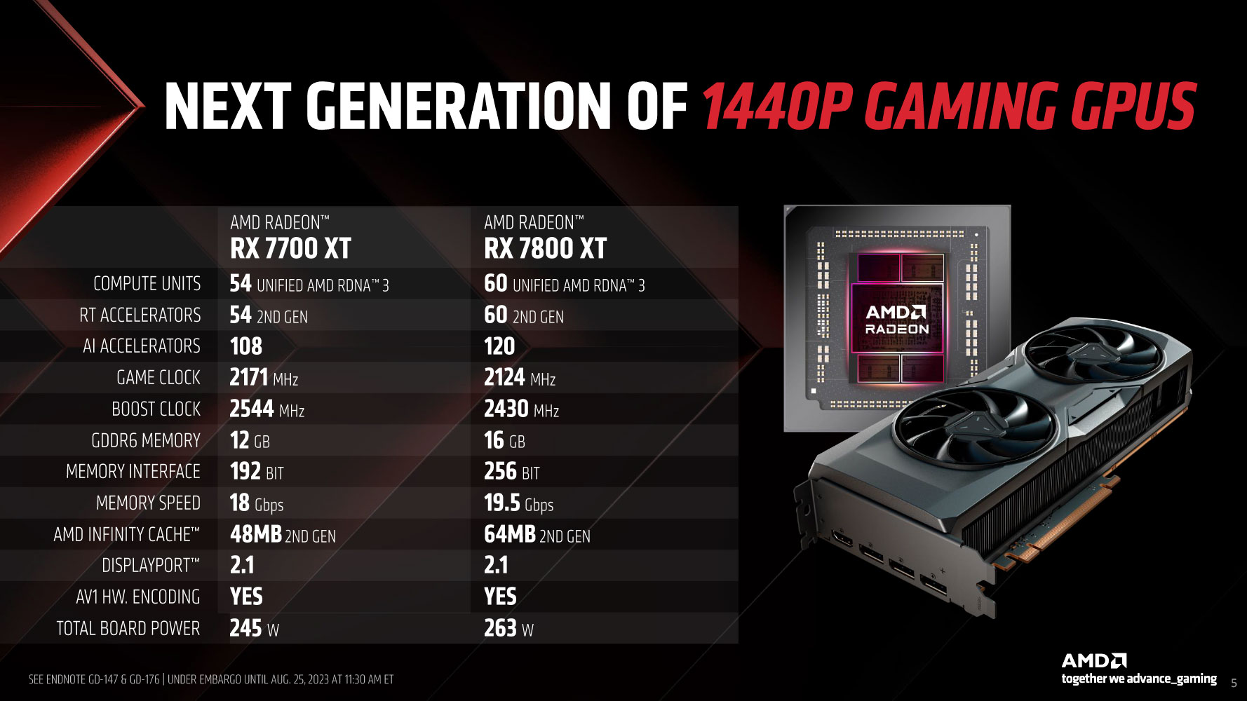
The Radeon RX 7800 XT and RX 7700 XT debut the new Navi 32 silicon, as part of AMD's desktop-first approach to the RX 7000 series. This is a chiplet-based GPU, just like the Navi 31 which powers the RX 7900 series, but scaled down. The centrally located graphics compute die (GCD) is based on the newer 5 nm EUV foundry process, and contains the main number crunching machinery of the GPU, all the stuff that tangibly benefits from the switch to the newer node, while the Infinity Cache and GDDR6 memory controllers—things that don't benefit as much from 5 nm, are spun off as chiplets called memory cache dies. Navi 32 gets four such MCDs compared to six on Navi 31. Each of these has a 16 MB segment of the GPU's 64 MB Infinity Cache, and a 64-bit portion of that adds up to its 256-bit GDDR6 memory interface.
The 5 nm GCD features 60 RDNA 3 compute units, each worth 64 stream processors, which works out to 3,840. This is a 50% generational increase in shaders compared to Navi 22 powering the Radeon RX 6700 series, but is a reduction when compared to the RX 6800 XT that's equipped with 72 RDNA 2 compute units. AMD is counting on the increased IPC, higher engine clocks, and greater memory bandwidth of Navi 32 to come through and make the RX 7800 XT faster than its predecessor; although given its pricing, AMD considers the RX 7800 XT to succeed the RX 5700 XT, and prove to be a viable upgrade for all those who held out on the RX 6000 series over the last three years.
The Radeon RX 7800 XT maxes out the Navi 32 silicon, enabling all 60 CUs, which work out to 3,840 stream processors, 120 AI accelerators, 60 Ray accelerators, 240 TMUs, and 96 ROPs. With all four MCDs enabled, the RX 7800 XT gets 64 MB of Infinity Cache, and a 256-bit GDDR6 memory interface, which it puts to good use with 16 GB of memory—same amount as the RX 6800 XT. The GPU runs at 2124 MHz Game clock, with 2420 MHz boost, however within this band internally, the front-end of the GPU runs at 10-15% higher clock speeds than the shader engines. The memory runs at 19.5 Gbps, which gives the RX 7800 XT a handy 628 GB/s of memory bandwidth.
The Radeon RX 7700 XT is cut down from the Navi 32 silicon, enabling 54 out of 60 CUs, giving it 3,456 stream processors, 108 AI accelerators, 54 Ray accelerators, 216 TMUs, and 96 ROPs. This SKU has three out of four MCDs enabled, which gives it 48 MB of Infinity Cache, and a 192-bit GDDR6 memory interface that is uses for its 12 GB of memory size. AMD runs the GPU at higher clock speeds than the RX 7800 XT, with 2171 MHz game clocks, and 2544 MHz boost. The memory is slightly slower, at 18 Gbps, giving it 432 GB/s of memory bandwidth.
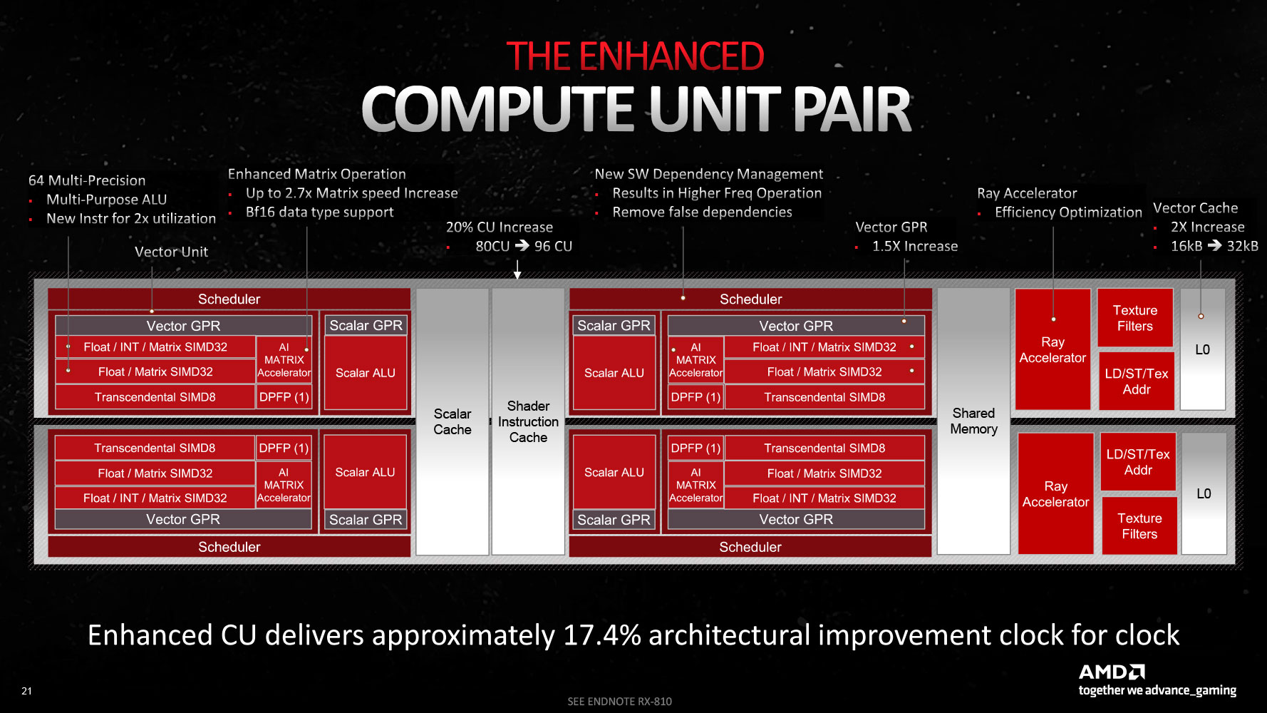
Much of the architectural innovation is this generation is with the RDNA 3 Dual-Compute Unit (or Compute Unit pair). The "Navi 32" GPU physically features 60 compute units spread across three Shader Engines. AMD claims that at the same engine clocks, the RDNA 3 CU offers a 17.4% IPC increase over the RDNA 2 CU.
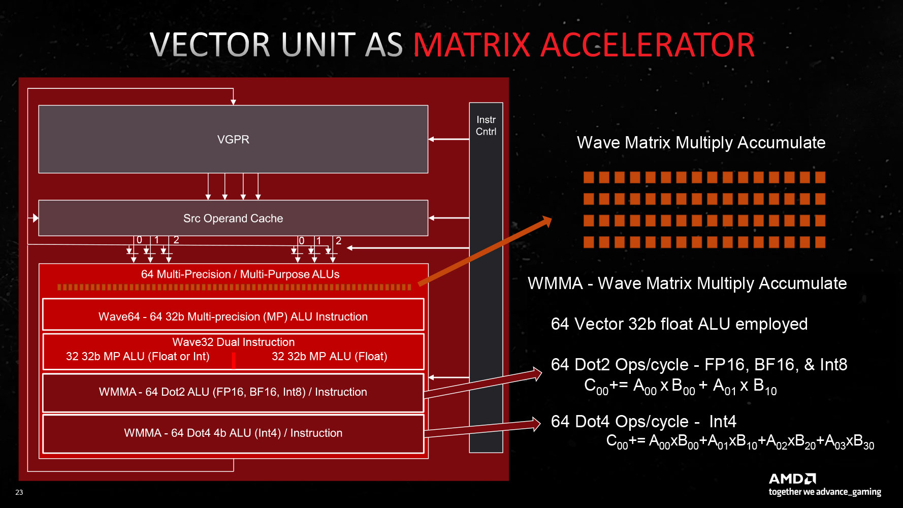
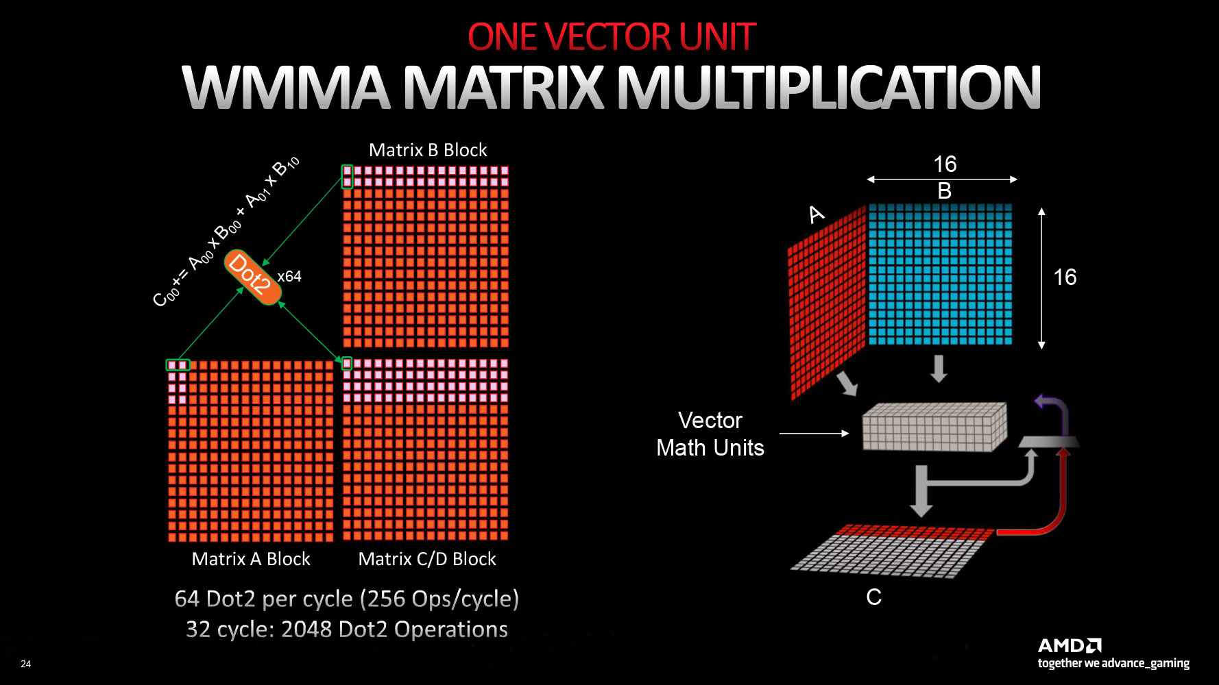
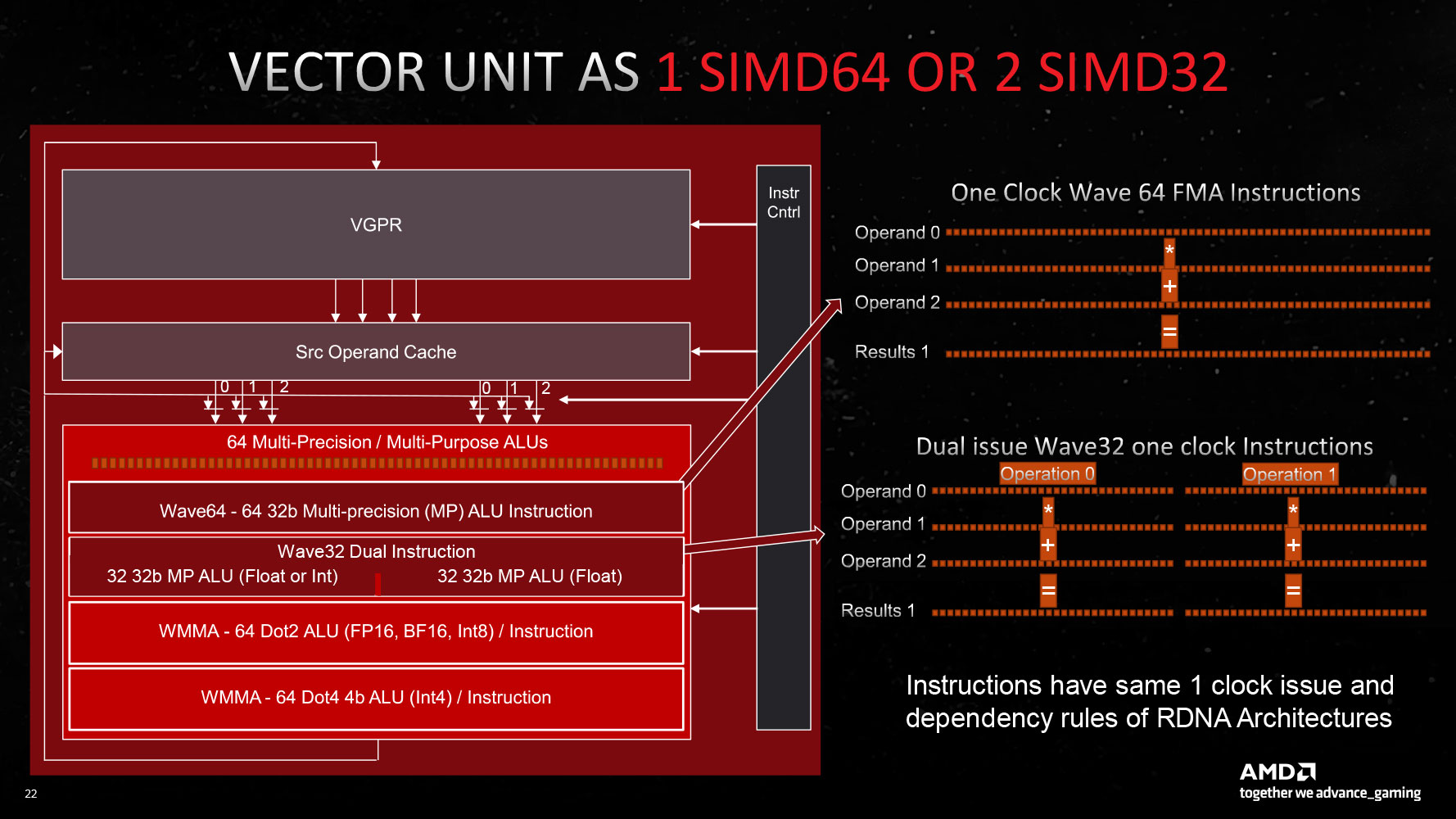
The new RDNA 3 CU introduces multi-precision capability for the 64 stream processors per CU: operating either as 1x SIMD64 or 2x SIMD32 units. The Vector Unit that houses these SIMD units can either function as a SIMD execution mechanism, or as a Matrix execution unit, thanks to the new AI Matrix Accelerator, which provides a 2.7x matrix multiplication performance uplift versus conventional SIMD execution. Also added are support for the Bfloat16 instruction-set, and SIMD8 execution. The GPU hence enjoys AI hardware-acceleration that can be leveraged in future feature-additions relevant to gamers. Game developers will also look for ways to exploit accelerated AI, now that all three brands feature it (NVIDIA Tensor cores and Intel XMX cores).
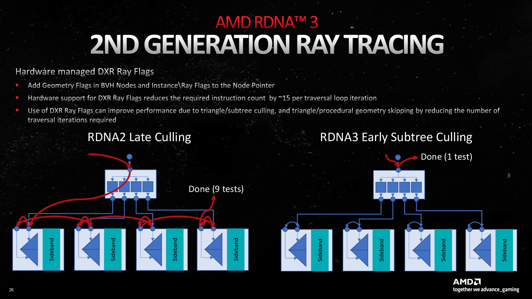
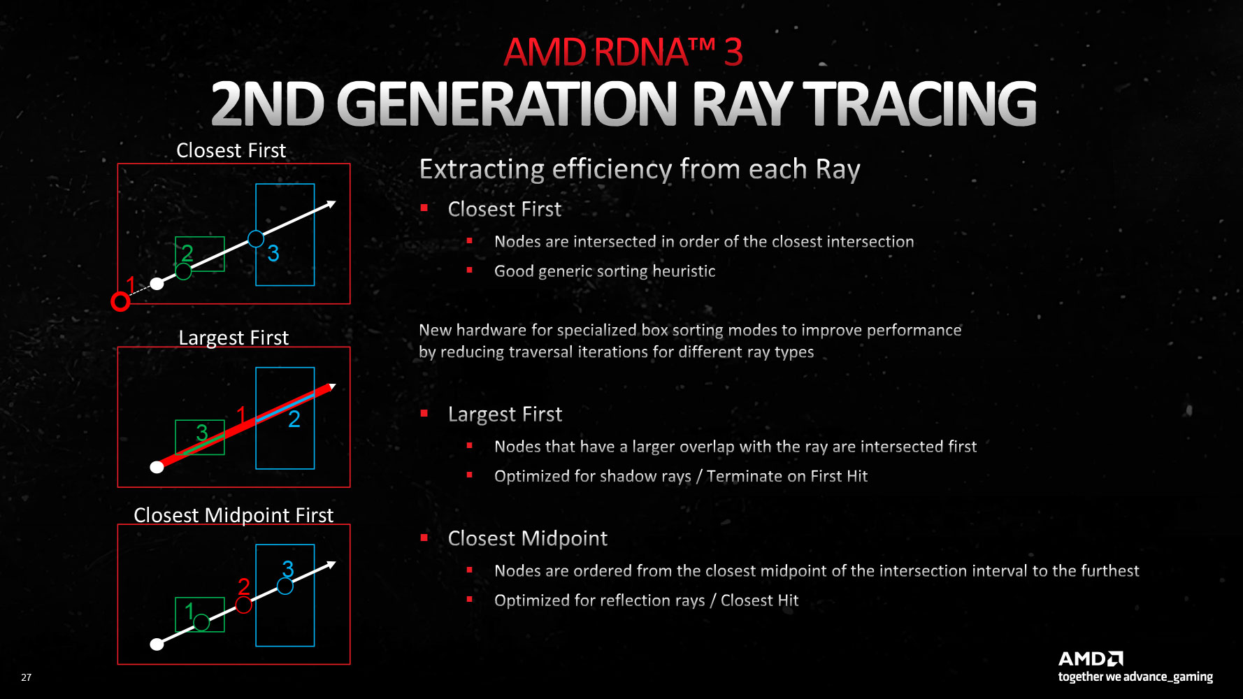
AMD's first-generation Ray Accelerator, introduced with the RDNA 2 architecture, was the result of a hasty effort to catch up to NVIDIA with a DirectX 12 Ultimate GPU, where they developed a fixed-function hardware to calculate ray intersections, and offloaded a large chunk of RT processing to the generationally-doubled SIMD resources. With RDNA 3, they've refined the Ray Accelerator to achieve an 80% ray tracing performance uplift over the previous generation, when you add up the Ray Accelerator count, their higher engine clocks, and other hardware-level optimizations, such as early sub-tree culling, specialized box sorting modes, and reduced traversal iterations.
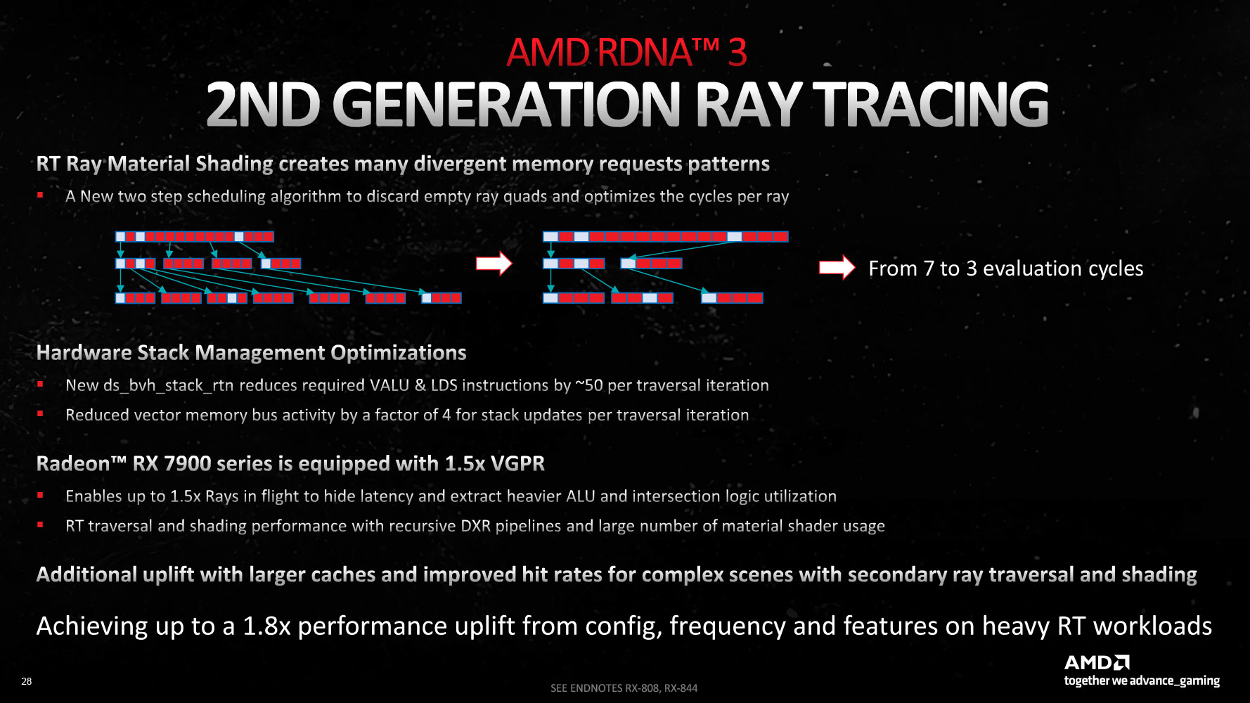
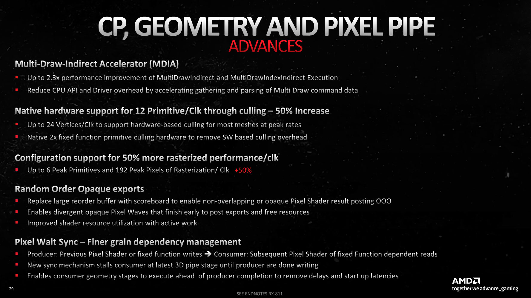
There is a 50% ray intersection capacity improvement for RDNA 3 thanks to these optimizations, and cycles-per-ray reduction. Besides these, AMD has also made several improvements to the geometry- and pixel-pipes, with the introduction of the new multi-draw indirect accelerator (MDIA), which reduces CPU API and driver-level overheads by gathering and parsing of multi-draw command data. At the hardware-level 12 primitives per clock is now supported compared to 8 per clock on RDNA 2, thanks to culling. The core-configuration overall enables 50% more rasterized performance per clock.

AMD has significantly improved the Display Engine of "Navi 32" over the previous-generation in terms of connectivity. The new Radiance Display Engine comes with native support for DisplayPort 2.1, which enables 8K output at up to 165 Hz refresh-rate, or 4K at up to 480 Hz, with a single cable. AMD has refined its FSR 2 algorithm to support 8K (i.e. render at a lower resolution with FSR-enhanced upscaling), to make it possible to enjoy the latest AAA titles at playable frame-rates on 8K displays. The RX 7800/7700 XT gets two full-size DP 2.1 connectors, besides an HDMI 2.1b, and a USB-C with DP 1.2 passthrough. The "Navi 32" silicon receives full hardware-accelerated AV1 encode and decode capabilities. With this generation, AMD is also introducing SmartAccess Video, a feature that lets the AMD driver leverage the hardware encoders of the RDNA 2 iGPU of Ryzen 7000 desktop processors, for additional encoding performance.
FidelityFX SuperResolution 3 Fluid Motion Frames (FSR 3 and FMF)
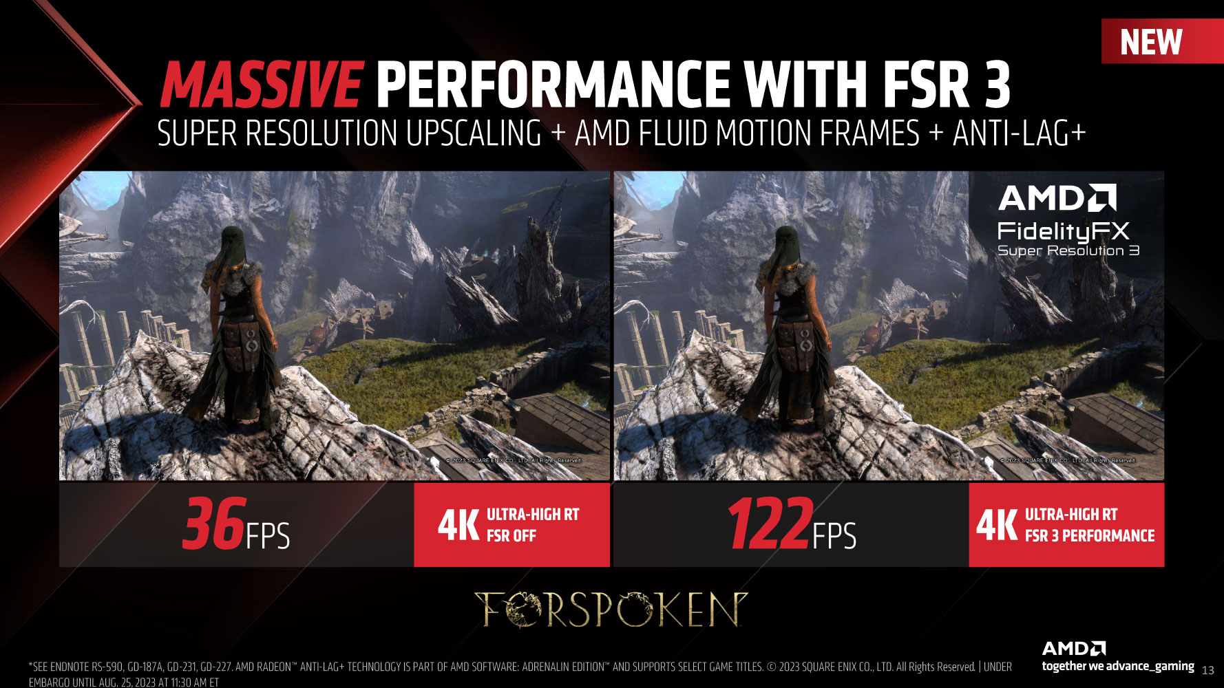
As part of the Radeon RX 7800 XT and RX 7700 XT announcements, AMD finally announced the much awaited FidelityFX Super Resolution 3 and Fluid Motion Frames. FSR 3 is being announced as a technological rival to NVIDIA DLSS 3 Frame Generation. The premise with both technologies is the same—to effectively double frame-rates by generating alternate frames without running them through the entire graphics rendering pipeline, it's just that the two technologies differ in their approach to this goal.
FSR 3 builds on FSR 2 with its updated super resolution upscaler promising generational quality improvements at a every given rendering resolution. Fluid Motion Frames (FMF) isn't the entirety of the FSR 3 feature-set, but is its most important feature-addition. FMF is a frame interpolation technology much like the one consumer televisions come with. Alternate frames are generated as an approximate of two frames. Where FMF differs from DLSS 3 Frame Generation is that while NVIDIA uses a hardware component called optical flow accelerator and the GPU's AI acceleration to generate an intermediate frame without involving the graphics rendering pipeline, FMF uses a certain amount of the graphics rendering pipeline. At a hardware level, FMF uses the main SIMD machinery of the GPU, leveraging asynchronous compute. As with DLSS 3 FG, FSR 3 FMF comes with added latency. NVIDIA counteracts this with Reflex, while AMD uses Radeon AntiLag+. Both technologies try to keep the frame queue short to reduce whole system latencies.
One major advantage FSR 3 FMF enjoys over DLSS 3 FG is that it works on any modern DirectX 12 GPU that supports async compute, since it doesn't require a specific hardware component the way DLSS 3 FG requires the Optical Flow Accelerator on NVIDIA "Ada" GPUs. The only limiting factor here is the performance. To be more specific, AMD says that all Radeon GPUs from RX 5700 series onward; and all GeForce GPUs from RTX 20-series onward, should support FSR 3 FMF. Also, FSR 3 FMF is as easy to integrate with games as FSR 2 is. The first games implementing FSR 3 FMF should arrive in Fall 2023. AMD is also working to extend FMF to Radeon Super Resolution, the driver-level technology that enables performance upscaling to even games that don't support FSR.
HYPR-RX

HYPR-RX is an interesting new feature AMD plans to integrate with the AMD Software (control center) application. It is a one-click performance boosting technology that works with any DirectX 11 or DirectX 12 game. The software is a cocktail of Radeon Boost, Radeon AntiLag+, and Radeon Super Resolution, and applies the three features on any running game as needed, automatically. Radeon Boost improves performance by dynamically reducing the render resolution of a game when there's too much motion on the screen (and hence not enough detail needed). Radeon Super Resolution improves frame-rates as it applies FSR on the output of a game rendered at a lower resolution (including the frames lowered in resolution by Radeon Boost. AntiLag+ counteracts the latency added by these two, by shortening the frame queue. AMD said that it is working to integrate FMF into the HYPR-RX feature-set.
Packaging


Our Patreon Silver Supporters can read articles in single-page format.
Apr 18th, 2025 09:30 EDT
change timezone
Latest GPU Drivers
New Forum Posts
- RX 9000 series GPU Owners Club (381)
- Overclocking an Intel I7-6700 (Non K) on a Lenovo 30L Gaming PC (13)
- The TPU UK Clubhouse (26143)
- Subsystem Id of my Asus Strix RTX 4090 OC / Random GPU detection problem (9)
- DTS DCH Driver for Realtek HDA [DTS:X APO4 + DTS Interactive] (2145)
- 5070 Ti power limit questions (50)
- Can anyone else replicate this crash on the 9070? (43)
- TPU's Rosetta Milestones and Daily Pie Thread (2280)
- Graphics cards for 1440p OLED - QD-OLED monitors. (12)
- Have you got pie today? (16670)
Popular Reviews
- ASUS GeForce RTX 5060 Ti TUF OC 16 GB Review
- NVIDIA GeForce RTX 5060 Ti PCI-Express x8 Scaling
- G.SKILL Trident Z5 NEO RGB DDR5-6000 32 GB CL26 Review - AMD EXPO
- Palit GeForce RTX 5060 Ti Infinity 3 16 GB Review
- ASUS GeForce RTX 5060 Ti Prime OC 16 GB Review
- Zotac GeForce RTX 5060 Ti AMP 16 GB Review
- MSI GeForce RTX 5060 Ti Gaming OC 16 GB Review
- Teevolution Terra Pro Review
- MSI GeForce RTX 5060 Ti Gaming Trio OC 16 GB Review
- ASUS GeForce RTX 5080 TUF OC Review
Controversial News Posts
- NVIDIA GeForce RTX 5060 Ti 16 GB SKU Likely Launching at $499, According to Supply Chain Leak (182)
- NVIDIA Sends MSRP Numbers to Partners: GeForce RTX 5060 Ti 8 GB at $379, RTX 5060 Ti 16 GB at $429 (127)
- Nintendo Confirms That Switch 2 Joy-Cons Will Not Utilize Hall Effect Stick Technology (105)
- Over 200,000 Sold Radeon RX 9070 and RX 9070 XT GPUs? AMD Says No Number was Given (100)
- Nintendo Switch 2 Launches June 5 at $449.99 with New Hardware and Games (99)
- NVIDIA Launches GeForce RTX 5060 Series, Beginning with RTX 5060 Ti This Week (97)
- Sony Increases the PS5 Pricing in EMEA and ANZ by Around 25 Percent (85)
- NVIDIA PhysX and Flow Made Fully Open-Source (77)