Tuesday, November 7th 2023

Intel "Emerald Rapids" 8592+ and 8558U Xeon CPUs with 64C and 48C Configurations Spotted

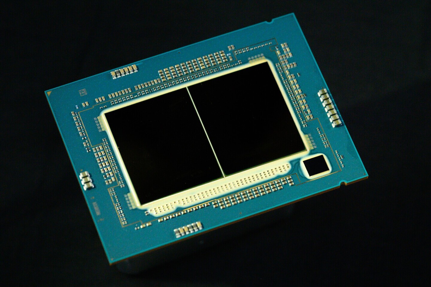
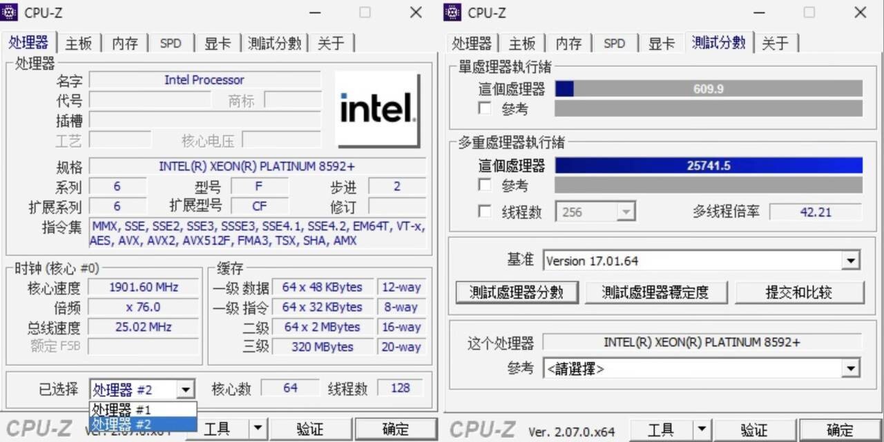
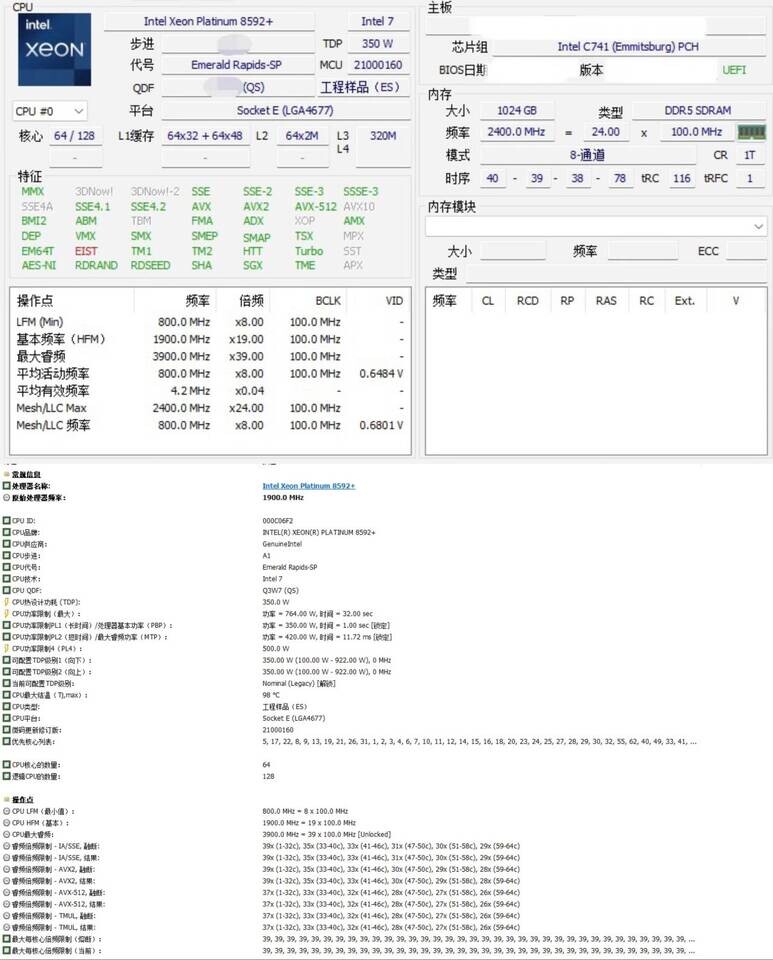
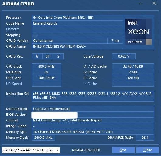
Intel's next-generation Emerald Rapids Xeon lineup is just around the corner, and we are now receiving more leaks as the launch nears. Today, we get to see leaks of two models: a 64-core Xeon 8592+ Platinum and a 48-core Xeon 8558U processor. First is the Xeon 8592+ Platinum, which is possibly Intel's top-end design with 64 cores and 128 threads. Running at the base frequency of 1.9 GHz, the CPU can boost up to 3.9 GHz. This SKU carries 488 MB of total cache, where 120 MB is dedicated to L2 and 320 MB is there for L3. With a TDP of 350 Watts, the CPU can even be adjusted to 420 Watts.

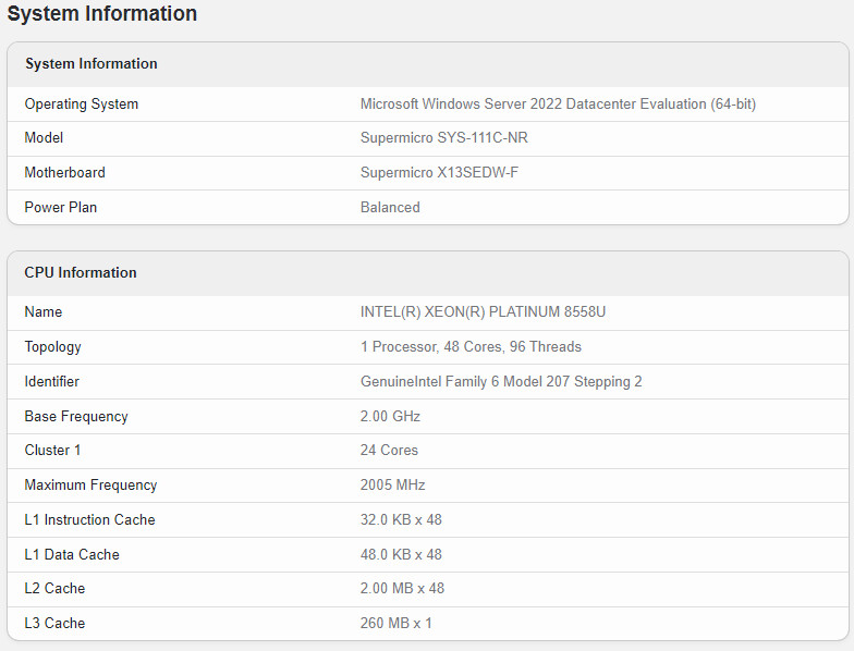
Next up, we have the Xeon 8558U processor, which has been spotted in Geekbench. The Xeon 8558U is a 48-core, 96-threaded CPU with a 2.0 GHz base clock whose boost frequency has yet to be shown or enabled, likely because it is an engineering sample. It carries 96 MB of L2 cache and 260 MB of L3 cache, making for a total of 356 MB of cache (which includes L1D and L1I as well). Both of these SKUs should launch with the remaining models in the Emerald Rapids family, dubbed 5th generation Xeon Scalable, on December 14 this year.
Sources: @792123a (X/Twitter), Geekbench, via VideoCardz
Add your own comment

19 Comments on Intel "Emerald Rapids" 8592+ and 8558U Xeon CPUs with 64C and 48C Configurations Spotted

#1
TumbleGeorge
In the material of one of the sources there is an interesting table listing the models. There is only one model marked "Gold", all others are "Platinum". However, I am interested in something else. About 1/3 of the models support DDR5 4800, other 1/3 - 5200 and last 1/3 - 5600 respectively. Is it possible that only the ones with DDR5 5600 support are actually "Emerald" architecture and the rest are rebranded older architectures?
Posted on Reply
#2
dj-electric
TumbleGeorgeIn the material of one of the sources there is an interesting table listing the models. There is only one model marked "Gold", all others are "Platinum". However, I am interested in something else. About 1/3 of the models support DDR5 4800, other 1/3 - 5200 and last 1/3 - 5600 respectively. Is it possible that only the ones with DDR5 5600 support are actually "Emerald" architecture and the rest are rebranded older architectures?
IMC rated DDR speeds are indeed very good indicator of a monolithic die's generational design.
By now, its not impossible Intel is combining 1st gen P-cores based IMC with 2nd gen and 2nd gen+ in one series.
Posted on Reply
#3
Daven
“This SKU carries 488 MB of total cache, where 120 MB is dedicated to L2 and 320 MB is there for L3.”

120 + 320 = 440

Besides it’s probably a misreport on the L2 cache which should be 2MB per core for 128 total. So we are looking at 448 MB of total L2+L3 cache in the 64 core part.
Posted on Reply
#4
TumbleGeorge
Daven“This SKU carries 488 MB of total cache, where 120 MB is dedicated to L2 and 320 MB is there for L3.”

120 + 320 = 440

Besides it’s probably a misreport on the L2 cache which should be 2MB per core for 128 total. So we are looking at 448 MB of total L2+L3 cache in the 64 core part.
Total means all levels of caches are in sum, include L1. Yes L2 is 128MB in slides.
Posted on Reply
#5
Daven
TumbleGeorgeTotal means all levels of caches are in sum, include L1. Yes L2 is 128MB in slides.
There is no way in hell there is 40MB of L1 cache. Besides Videocardz is reporting 448 MB. Its just a typo in the article.

Edit: Look like 80 KB of L1 Cache per core
128+320+5= 453 MB total cache
Posted on Reply
#6
Shtb
2 dies instead of 4? How come Intel, since it's so easy to implement, it's just "glued together"?
Posted on Reply
#7
TumbleGeorge
Daven128+320+5= 453 MB total cache
I wonder if it also applies to the cache how much is the actual printed size, and how much is reported by the OS and how much of the caches capacity is actually usable by the user's applications?
Posted on Reply
#8
Daven
TumbleGeorgeI wonder if it also applies to the cache how much is the actual printed size, and how much is reported by the OS and how much of the caches capacity is actually usable by the user's applications?
I think @AleksanderK just made a couple of typos. The L2 Cache is 128 MB and the total L2+L3 cache is 448 MB. Usually L1 cache is not used when reporting total cache size.

As for your comment, usually the amounts of cache shown in CPUz is the amount available to the OS and applications. I am not aware of any overhead, provisioning or otherwise hidden cache.

Edit: I should mention that @AleksanderK only made one typo. The 488 should say 448. The 120 typo is carried over from a typo in the original Videocardz article.
Posted on Reply
#9
TumbleGeorge
I think that maybe have around 10% spare cache to hot replace of defective cache blocks. Or I'm wrong?
Posted on Reply
#12
lemonadesoda
^ doesnt look right. Multicore only 10x faster but 48 cores/96 threads. I would expect a different scale statistic unless they are choking to death due to downclocking and/or cache incoherence/starvation. Quick google search gives me:
The multi-core benchmark tests in Geekbench 6 have also undergone a significant overhaul. Rather than assigning separate tasks to each core, the tests now measure how cores cooperate to complete a shared task.
The new "shared task" approach requires cores to co-operate by sharing information. Given the larger datasets used in Geekbench 6 several workloads are now memory-constrained, rather than CPU-constrained, on most systems.
Not sure GB6 is at all useful for high core CPUs, since, by purpose, high core CPUs are designed to run multiple separate and independent tasks.
Posted on Reply
#13
AnotherReader
TumbleGeorgeI think that maybe have around 10% spare cache to hot replace of defective cache blocks. Or I'm wrong?
That would be rather wasteful of die space. In the past, much smaller ratios have been used. Over 20 years ago, Intel used less than 2% of the L3 cache's actual capacity for redundancy:
The McKinley’s L3 is composed of 135 identical 24 KB sub-blocks. Of these, 128 are used to store data, 5 are used to hold EDC check bits, and 2 are used for redundancy.
Posted on Reply
#15
AnotherReader
TumbleGeorgeWell, downsizing over the past period may have made the components less durable despite all measures to protect them.
This redundancy was to account for manufacturing defects; durability for servers running at near constant load shouldn't be a concern. The power density is much less than even a 12600K on the same process and it won't suffer from thermal cycling to the same extent as a typical consumer CPU. At least for TSMC, defect density has improved or held steady for new processes. Of course, only Intel and some of its foundry customers know what Intel's defect rate is.
Posted on Reply
#16
TumbleGeorge
AnotherReaderThis redundancy was to account for manufacturing defects; durability for servers running at near constant load shouldn't be a concern. The power density is much less than even a 12600K on the same process and it won't suffer from thermal cycling to the same extent as a typical consumer CPU. At least for TSMC, defect density has improved or held steady for new processes. Of course, only Intel and some of its foundry customers know what Intel's defect rate is.
I didn't even mean the density of defects in production, only those occurring in use. Although defectively manufactured components also occupy some area. This is the state of things. The physics of microscale materials is killer the lower you go.
Posted on Reply
#17
AnotherReader
TumbleGeorgeI didn't even mean the density of defects in production, only those occurring in use. Although defectively manufactured components also occupy some area. This is the state of things. The physics of microscale materials is killer the lower you go.
Luckily, this is digital logic so variation in threshold voltages, and circuit resistance or capacitance is relatively easily accommodated.
Posted on Reply
#18
Wirko
That 8558Uranium must sit somewhere between the i7-8550U and the i7-8559U, hah.

More seriously, the "U" apparently means a processor without UPI interprocessor links, at least in Sapphire Rapids generation, therefore not able to work in multiprocessor systems.
TumbleGeorgeI didn't even mean the density of defects in production, only those occurring in use. Although defectively manufactured components also occupy some area. This is the state of things. The physics of microscale materials is killer the lower you go.
Static RAM, or dynamic RAM for that matter, can't be compared to NAND, which wears out with use. Any defects in RAM must be detected in the chip testing phase, and worked around once and for all, if at all possible. It is not known how Intel and others correct the defects. Maybe they make use of redundant cache lines. The other option is to just tag the defective cache lines and exclude them from use, so you get 35.992 MiB of L3 for the price of 36 MiB. The OS and applications know nothing about that, it's only the cache controller's business.

But ... if there are several defects in the L3 area, it means that there are defects everywhere, and it's nearly impossible for the rest of the chip to be defect-free. So, while it's useful to have a little bit of redundancy and save some nice costly chips from recycling, it's not useful to have a lot of it.
Posted on Reply
#19
Jism
Can someone compare those scores vs a Epyc at the same threads/cores please?

I'm pretty sure the Epyc would be overall better due to it's more efficient design. the sapphire has bin plagued.
Posted on Reply
Add your own comment
May 21st, 2024 06:30 EDT change timezone

New Forum Posts

Popular Reviews

Controversial News Posts