Wednesday, February 21st 2024

Intel Xeon "Granite Rapids" Wafer Pictured—First Silicon Built on Intel 3

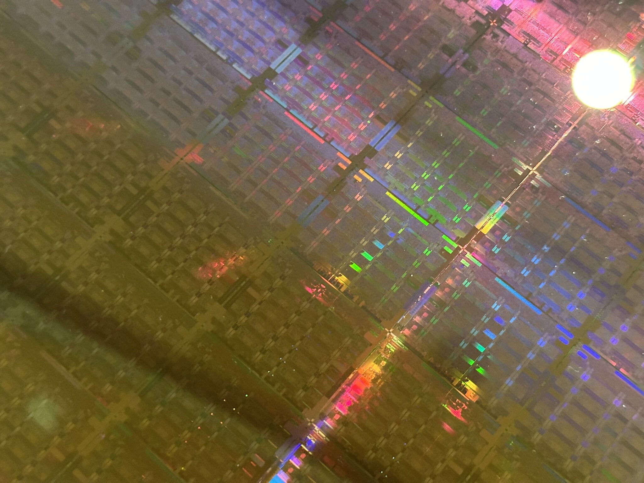
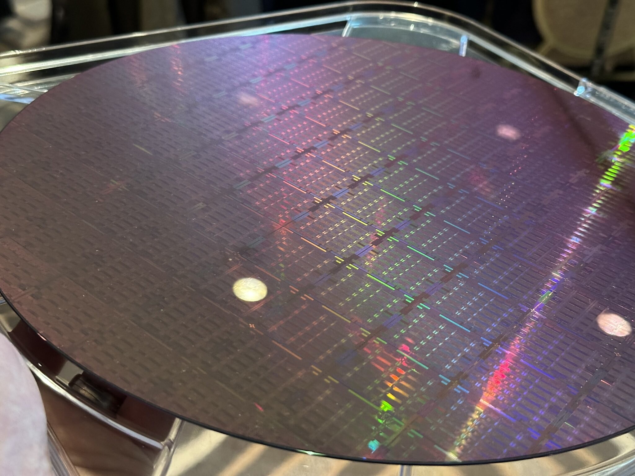
Feast your eyes on the first pictures of an Intel "Granite Rapids" Xeon processor wafer, courtesy of Andreas Schilling with HardwareLuxx.de. This is Intel's first commercial silicon built on the new Intel 3 foundry node, which is expected to be the company's final silicon fabrication node to implement FinFET technology; before the company switches to Nanosheets with the next-generation Intel 20A. Intel 3 offers transistor densities and performance competitive to TSMC N3 series, and Samsung 3GA series nodes.

The wafer contains square 30-core tiles, two of which make up a "Granite Rapids-XCC" processor, with CPU core counts going up to 56-core/112-threads (two cores left unused per tile for harvesting). Each of the 30 cores on the tile is a "Redwood Cove" P-core. In comparison, the current "Emerald Rapids" Xeon processor uses "Raptor Cove" cores, and is built on the Intel 7 foundry node. Intel is planning to overcome the CPU core-count deficit to AMD EPYC, including the upcoming EPYC "Turin" Zen 5 processors with their rumored 128-core/256-thread counts, by implementing several on-silicon fixed-function accelerators that speed up popular kinds of server workloads. The "Redwood Cove" core is expected to be Intel's first IA core to implement AVX10 and APX.
Source: Andreas Schilling (Twitter)
Add your own comment

18 Comments on Intel Xeon "Granite Rapids" Wafer Pictured—First Silicon Built on Intel 3

#1
docnorth
Is Intel 3 technically still a 7nm node with improved density and properties? It's a real question, thanks.
Posted on Reply
#3
JAKra
Those are HUGE chips/tiles!
They need 2 of those for top-end Xeon, right? I presume these are quite expensive wafers.
Even if all chips have 0 defects (impossible) you can make around 30-40 top-end CPUs from one wafer?
Posted on Reply
#4
dgianstefani
TPU Proofreader
docnorthIs Intel 3 technically still a 7nm node with improved density and properties? It's a real question, thanks.
nm ratings aren't real, just marketing approximations of technology level. This goes for TSMC and Samsung too.

Compare density, frequency and power performance, not nm.
Posted on Reply
#5
Daven
dgianstefaninm ratings aren't real, just marketing approximations of technology level. This goes for TSMC and Samsung too.

Compare density, frequency and power performance, not nm.
Easier said than done. These numbers are very hard to come by with certainty.
Posted on Reply
#6
dgianstefani
TPU Proofreader
DavenEasier said than done. These numbers are very hard to come by with certainty.
www.techpowerup.com/cpu-specs/

Our database has detailed info. Weighing transistors/die size is a simple way of figuring out density.

Posted on Reply
#7
Denver
Oh, intel 3 exists. Now show the product working.
Posted on Reply
#8
Daven
dgianstefaniwww.techpowerup.com/cpu-specs/

Our database has detailed info. Weighing transistors/die size is a simple way of figuring out density.

I’ve had issues with the TPU database using placeholder values based on ‘leaked’ or ‘rumored’ information before the actual product launch and then not updating when the actual numbers come out. For example, the entry for the MI300X was totally wrong and these wrong numbers made it into a front page article after launch. The numbers have been fixed since I pointed out the error.

Don’t get me wrong, I love databases like the one at TPU but the website has to have the personnel to keep it accurate which is not an easy thing to do or have the money for a dedicated job position.

Edit: And your screen capture is for a specific CPU, not the highest density capabilities of a fab node. They are not always one in the same. Case in point, Zen 4 vs Zen 4c, same node but different densities.

Edit2: Also there are different versions of the same node. TPU still uses the old ‘plus’ sign moniker as in the upcoming hardware launches article and not the actual node names such as N4, N4P, N4X for the different TSMC 4 nm nodes for example. This info is also hard to come by and changes the density values. There is no such thing as ‘plus’ anymore.
Posted on Reply
#9
Denver
DavenI’ve had issues with the TPU database using placeholder values based on ‘leaked’ or ‘rumored’ information before the actual product launch and then not updating when the actual numbers come out. For example, the entry for the MI300X was totally wrong and these wrong numbers made it into a front page article after launch. The numbers have been fixed since I pointed out the error.

Don’t get me wrong, I love databases like the one at TPU but the website has to have the personnel to keep it accurate which is not an easy thing to do or have the money for a dedicated job position.

Edit: And your screen capture is for a specific CPU, not the highest density capabilities of a fab node. They are not always one in the same. Case in point, Zen 4 vs Zen 4c, same node but different densities.
Generally, smaller caches lead to higher transistor density. However, the density figures published by fabs can be unrealistic at times because the reference chips they use may differ significantly from commercial products. Conveniently, Intel has recently stopped disclosing transistor count info on their CPUs. Guess why
Posted on Reply
#10
AnarchoPrimitiv
I imagine that using weight and volume to figure out density is difficult without extremely precise scales AND being able to weigh individual chiplets detached from interposers and other chipsets
Posted on Reply
#11
Frank_100
dgianstefaninm ratings aren't real, just marketing approximations of technology level. This goes for TSMC and Samsung too.

Compare density, frequency and power performance, not nm.
An engineer can explain it.
Posted on Reply
#12
docnorth
dgianstefaninm ratings aren't real, just marketing approximations of technology level. This goes for TSMC and Samsung too.

Compare density, frequency and power performance, not nm.
Yes I've learned that from the Coffee Lake vs Zen era, e.g. 8700(K) vs ryzen 2700x (more experienced members probably knew this long ago). Hence the term technically, I'm still curious, but it is also good to know if a node has further margins of improvement or has reached it's limits.
Posted on Reply
#13
AMDK11
There are physically 33 cores on the board. 4 rows of 7 cores and 1 row of 5 cores.

This is not GraniteRapids!

The photos show EmeraldRapids with physically 33 RaptorCove cores.
Posted on Reply
#14
AnotherReader
docnorthYes I've learned that from the Coffee Lake vs Zen era, e.g. 8700(K) vs ryzen 2700x (more experienced members probably knew this long ago). Hence the term technically, I'm still curious, but it is also good to know if a node has further margins of improvement or has reached it's limits.
In addition, the industry often publishes relevant process details such as gate pitch, fin height, and the various metal layer pitches. An analysis of these reveals that Intel 4 is closer to TSMC's N3 than N5.
Posted on Reply
#15
JohH
docnorthIs Intel 3 technically still a 7nm node with improved density and properties? It's a real question, thanks.
No, Intel 4 is what Intel was calling 7nm. But it is higher density compared to other companies "7nm" processes. Indeed it is closer to N5 or even N4. Hence the name change.
Posted on Reply
#16
Wirko
ReadlightWhy shines in many colors?
Because the transistor size is much closer to the wavelengths of visible light than the oligopoly says aloud.
AMDK11There are physically 33 cores on the board. 4 rows of 7 cores and 1 row of 5 cores.

This is not GraniteRapids!

The photos show EmeraldRapids with physically 33 RaptorCove cores.
Yes. the die size also checks out, it's roughly 25 x 30 mm.
Posted on Reply
#17
AnotherReader
WirkoBecause the transistor size is much closer to the wavelengths of visible light than the oligopoly says aloud.


Yes. the die size also checks out, it's roughly 25 x 30 mm.
The naming never reflected transistor size. For a long time, it was the minimum feature size, typically gate length or half of minimum metal pitch. Wikichip's summary is accurate:
Historically, the process node name referred to a number of different features of a transistor including the gate length as well as M1 half-pitch. Most recently, due to various marketing and discrepancies among foundries, the number itself has lost the exact meaning it once held. Recent technology nodes such as 22 nm, 16 nm, 14 nm, and 10 nm refer purely to a specific generation of chips made in a particular technology. It does not correspond to any gate length or half pitch. Nevertheless, the name convention has stuck and it's what the leading foundries call their nodes.

Since around 2017 node names have been entirely overtaken by marketing with some leading-edge foundries using node names ambiguously to represent slightly modified processes. Additionally, the size, density, and performance of the transistors among foundries no longer matches between foundries. For example, Intel's 10 nm is comparable to foundries 7 nm while Intel's 7 nm is comparable to foundries 5 nm.
Posted on Reply
#18
Minus Infinity
Intel Granite Rapids and AMD Granite Ridge in the same year.
Posted on Reply
Add your own comment
May 21st, 2024 19:09 EDT change timezone

New Forum Posts

Popular Reviews

Controversial News Posts