Wednesday, February 21st 2024

Intel Announces Intel 14A (1.4 nm) and Intel 3T Foundry Nodes, Launches World's First Systems Foundry Designed for the AI Era
Intel Corp. today launched Intel Foundry as a more sustainable systems foundry business designed for the AI era and announced an expanded process roadmap designed to establish leadership into the latter part of this decade. The company also highlighted customer momentum and support from ecosystem partners - including Synopsys, Cadence, Siemens and Ansys - who outlined their readiness to accelerate Intel Foundry customers' chip designs with tools, design flows and IP portfolios validated for Intel's advanced packaging and Intel 18A process technologies.
The announcements were made at Intel's first foundry event, Intel Foundry Direct Connect, where the company gathered customers, ecosystem companies and leaders from across the industry. Among the participants and speakers were U.S. Secretary of Commerce Gina Raimondo, Arm CEO Rene Haas, Microsoft CEO Satya Nadella, OpenAI CEO Sam Altman and others. "AI is profoundly transforming the world and how we think about technology and the silicon that powers it," said Intel CEO Pat Gelsinger. "This is creating an unprecedented opportunity for the world's most innovative chip designers and for Intel Foundry, the world's first systems foundry for the AI era. Together, we can create new markets and revolutionize how the world uses technology to improve people's lives."
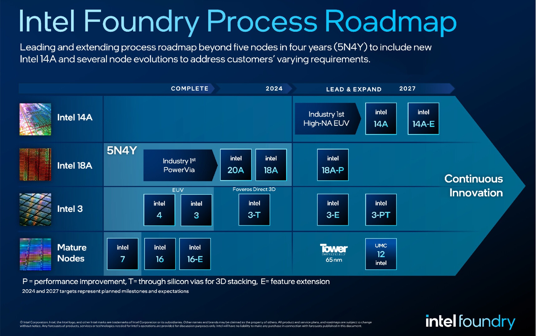
Process Roadmap Expands Beyond 5N4Y
Intel's extended process technology roadmap adds Intel 14A to the company's leading-edge node plan, in addition to several specialized node evolutions. Intel also affirmed that its ambitious five-nodes-in-four-years (5N4Y) process roadmap remains on track and will deliver the industry's first backside power solution. Company leaders expect Intel will regain process leadership with Intel 18A in 2025.
The new roadmap includes evolutions for Intel 3, Intel 18A and Intel 14A process technologies. It includes Intel 3-T, which is optimized with through-silicon vias for 3D advanced packaging designs and will soon reach manufacturing readiness. Also highlighted are mature process nodes, including new 12 nanometer nodes expected through the joint development with UMC announced last month. These evolutions are designed to enable customers to develop and deliver products tailored to their specific needs. Intel Foundry plans a new node every two years and node evolutions along the way, giving customers a path to continuously evolve their offerings on Intel's leading process technology.
Intel also announced the addition of Intel Foundry FCBGA 2D+ to its comprehensive suite of ASAT offerings, which already include FCBGA 2D, EMIB, Foveros and Foveros Direct.
Microsoft Design on Intel 18A Headlines Customer Momentum
Customers are supporting Intel's long-term systems foundry approach. During Pat Gelsinger's keynote, Microsoft Chairman and CEO Satya Nadella stated that Microsoft has chosen a chip design it plans to produce on the Intel 18A process.
"We are in the midst of a very exciting platform shift that will fundamentally transform productivity for every individual organization and the entire industry," Nadella said. "To achieve this vision, we need a reliable supply of the most advanced, high-performance and high-quality semiconductors. That's why we are so excited to work with Intel Foundry, and why we have chosen a chip design that we plan to produce on Intel 18A process."
Intel Foundry has design wins across foundry process generations, including Intel 18A, Intel 16 and Intel 3, along with significant customer volume on Intel Foundry ASAT capabilities, including advanced packaging.
In total, across wafer and advanced packaging, Intel Foundry's expected lifetime deal value is greater than $15 billion.
IP and EDA Vendors Declare Readiness for Intel Process and Packaging Designs
Intellectual property and electronic design automation (EDA) partners Synopsys, Cadence, Siemens, Ansys, Lorentz and Keysight disclosed tool qualification and IP readiness to enable foundry customers to accelerate advanced chip designs on Intel 18A, which offers the foundry industry's first backside power solution. These companies also affirmed EDA and IP enablement across Intel node families.
At the same time, several vendors announced plans to collaborate on assembly technology and design flows for Intel's embedded multi-die interconnect bridge (EMIB) 2.5D packaging technology. These EDA solutions will ensure faster development and delivery of advanced packaging solutions for foundry customers.
Intel also unveiled an "Emerging Business Initiative" that showcases a collaboration with Arm to provide cutting-edge foundry services for Arm-based system-on-chips (SoCs). This initiative presents an important opportunity for Arm and Intel to support startups in developing Arm-based technology and offering essential IP, manufacturing support and financial assistance to foster innovation and growth.
Systems Approach Differentiates Intel Foundry in the AI Era
Intel's systems foundry approach offers full-stack optimization from the factory network to software. Intel and its ecosystem empower customers to innovate across the entire system through continuous technology improvements, reference designs and new standards.
Stuart Pann, senior vice president of Intel Foundry at Intel said, "We are offering a world-class foundry, delivered from a resilient, more sustainable and secure source of supply, and complemented by unparalleled systems of chips capabilities. Bringing these strengths together gives customers everything they need to engineer and deliver solutions for the most demanding applications."
Global, Resilient, More Sustainable and Trusted Systems Foundry
Resilient supply chains must also be increasingly sustainable, and today Intel shared its goal of becoming the industry's most sustainable foundry. In 2023, preliminary estimates show that Intel used 99% renewable electricity in its factories worldwide. Today, the company redoubled its commitment to achieving 100% renewable electricity worldwide, net-positive water and zero waste to landfills by 2030. Intel also reinforced its commitment to net-zero Scope 1 and Scope 2 GHG emissions by 2040 and net-zero upstream Scope 3 emissions by 2050.
The announcements were made at Intel's first foundry event, Intel Foundry Direct Connect, where the company gathered customers, ecosystem companies and leaders from across the industry. Among the participants and speakers were U.S. Secretary of Commerce Gina Raimondo, Arm CEO Rene Haas, Microsoft CEO Satya Nadella, OpenAI CEO Sam Altman and others.
Process Roadmap Expands Beyond 5N4Y
Intel's extended process technology roadmap adds Intel 14A to the company's leading-edge node plan, in addition to several specialized node evolutions. Intel also affirmed that its ambitious five-nodes-in-four-years (5N4Y) process roadmap remains on track and will deliver the industry's first backside power solution. Company leaders expect Intel will regain process leadership with Intel 18A in 2025.
The new roadmap includes evolutions for Intel 3, Intel 18A and Intel 14A process technologies. It includes Intel 3-T, which is optimized with through-silicon vias for 3D advanced packaging designs and will soon reach manufacturing readiness. Also highlighted are mature process nodes, including new 12 nanometer nodes expected through the joint development with UMC announced last month. These evolutions are designed to enable customers to develop and deliver products tailored to their specific needs. Intel Foundry plans a new node every two years and node evolutions along the way, giving customers a path to continuously evolve their offerings on Intel's leading process technology.
Intel also announced the addition of Intel Foundry FCBGA 2D+ to its comprehensive suite of ASAT offerings, which already include FCBGA 2D, EMIB, Foveros and Foveros Direct.
Microsoft Design on Intel 18A Headlines Customer Momentum
Customers are supporting Intel's long-term systems foundry approach. During Pat Gelsinger's keynote, Microsoft Chairman and CEO Satya Nadella stated that Microsoft has chosen a chip design it plans to produce on the Intel 18A process.
"We are in the midst of a very exciting platform shift that will fundamentally transform productivity for every individual organization and the entire industry," Nadella said. "To achieve this vision, we need a reliable supply of the most advanced, high-performance and high-quality semiconductors. That's why we are so excited to work with Intel Foundry, and why we have chosen a chip design that we plan to produce on Intel 18A process."
Intel Foundry has design wins across foundry process generations, including Intel 18A, Intel 16 and Intel 3, along with significant customer volume on Intel Foundry ASAT capabilities, including advanced packaging.
In total, across wafer and advanced packaging, Intel Foundry's expected lifetime deal value is greater than $15 billion.
IP and EDA Vendors Declare Readiness for Intel Process and Packaging Designs
Intellectual property and electronic design automation (EDA) partners Synopsys, Cadence, Siemens, Ansys, Lorentz and Keysight disclosed tool qualification and IP readiness to enable foundry customers to accelerate advanced chip designs on Intel 18A, which offers the foundry industry's first backside power solution. These companies also affirmed EDA and IP enablement across Intel node families.
At the same time, several vendors announced plans to collaborate on assembly technology and design flows for Intel's embedded multi-die interconnect bridge (EMIB) 2.5D packaging technology. These EDA solutions will ensure faster development and delivery of advanced packaging solutions for foundry customers.
Intel also unveiled an "Emerging Business Initiative" that showcases a collaboration with Arm to provide cutting-edge foundry services for Arm-based system-on-chips (SoCs). This initiative presents an important opportunity for Arm and Intel to support startups in developing Arm-based technology and offering essential IP, manufacturing support and financial assistance to foster innovation and growth.
Systems Approach Differentiates Intel Foundry in the AI Era
Intel's systems foundry approach offers full-stack optimization from the factory network to software. Intel and its ecosystem empower customers to innovate across the entire system through continuous technology improvements, reference designs and new standards.
Stuart Pann, senior vice president of Intel Foundry at Intel said, "We are offering a world-class foundry, delivered from a resilient, more sustainable and secure source of supply, and complemented by unparalleled systems of chips capabilities. Bringing these strengths together gives customers everything they need to engineer and deliver solutions for the most demanding applications."
Global, Resilient, More Sustainable and Trusted Systems Foundry
Resilient supply chains must also be increasingly sustainable, and today Intel shared its goal of becoming the industry's most sustainable foundry. In 2023, preliminary estimates show that Intel used 99% renewable electricity in its factories worldwide. Today, the company redoubled its commitment to achieving 100% renewable electricity worldwide, net-positive water and zero waste to landfills by 2030. Intel also reinforced its commitment to net-zero Scope 1 and Scope 2 GHG emissions by 2040 and net-zero upstream Scope 3 emissions by 2050.
45 Comments on Intel Announces Intel 14A (1.4 nm) and Intel 3T Foundry Nodes, Launches World's First Systems Foundry Designed for the AI Era
AMD's GCD in Navi 31: 304.35 mm2 45.4B transistors - that's 150.2 MTr / mm2 or 176.7 Mtr / mm2 for the TSMC 5 nm.
Wikipedia states something very weird:
TSMC 5 nm = 138.2 MTr / mm2
TSMC 3 nm = 224.2 Mtr / mm2
now 2024 is supposed to be the year when 20A (3NM old) is released in mass volume for the CPU tile
How is that even possible they skipped the old 7 and 4. will be used for other tiles but still.
7nm TSMC Compute die
~76 mm2
3.8B xtors
50 MTr/mm2
Zen 3
7nm TSMC Compute die
~84 mm2
4.15B xtors
49.40 MTr/mm2
Zen 4
5nm TSMC Compute die
~71 mm2
6.57B xtors
92.54 MTr/mm2
Also Intel 3 is just improved Intel 4 and they both are what used to be named 7nm. 20A and 18A will be what used to be 5nm and 14A what used to be 3nm. All these names are just marketing.
The GTX 580 (40nm) was 520mm2 @ 3B transistors. As the cache is always less dense, expect something like twice the size, 1040mm. Therefore, a silicon notebook, rather than a GPU. Useless... Moreover, the inter-die connection technology required would likely be impractical or non-functional.
The MCM design makes the chip a little more inefficient. However, the N31's problem is more about software than hardware. Nvidia extends its tentacles, putting engineers working in every possible studio, even indies, to make everything run better on its hardware. AMD dealing with Intel and Nvidia at the same time cannot do this to the same degree.
Navi 31's MCD is 225.12 mm2, that made on a 14 nm process would be equivalent to 489 mm2.
If AMD was smart, decrease the Infinity cache size and make the MCD using the older process.
Wafer prices - < 3000$ for 14 nm
Wafer prices - between 9000 and 10000$ for 6 nm.
It is a brilliant idea.
Actually, TBH, if AMD had those "brilliant minds", it wouldn't be in that situation it is in now.
Then... Yes, following your ideas is useless. :rolleyes:
You state the cost of 1 MCD. They put 6 of them - that's at least 42$.
Also, unite those cut 6 MCD into a single die on a 14 nm.
There is a reason why the RAM manufacturers use 1x nodes, not 7 nm. :rolleyes:
SRAM; Uses flip-flops to store each bit of data. A flip-flop consists of several logic gates that maintain their state (0 or 1) as long as power is maintained.
DDR RAM: Uses storage cells based on capacitors and transistors to store bits. Each cell contains a capacitor that stores electrical charge to represent a bit.
"Some news for Sapphire Rapids from ISSCC: According to Nevine Nassif, Principal Engineer for Sapphire Rapids at Intel, the die size is a little lower than 400 mm² and the transistor count is between 11 and 12 billion."
Intel 7(E10SF)
"Some news for Sapphire Rapids from ISSCC: According to Nevine Nassif, Principal Engineer for Sapphire Rapids at Intel, the die size is a little lower than 400 mm² and the transistor count is between 11 and 12 billion."
Where did the 26 billion transistors in RaptorLake-S come from?
Intel 7 is definitely not 100 MTr/mm2.
SapphireRapids is 4x400 mm2, giving a total of 1600 mm2 and 46 billion transistors for physically 60 cores.
Genoa has 96 cores, i.e. 12 chiplets of 8 cores each + I/O chiplet.
Two 2x 71 mm2 dies and 6.57 billion transistors give a total of 142 mm2 for 16 cores (Zen 4) and 13.14 billion transistors + I/O chiplet.
Can TSMC Maintain Their Process Technology Lead - SemiWiki
EmeraldRapids physically has 2x 33 cores for a total of 66 cores with LLC per single 5MB core instead of 1.875MB (SapphireRapids).
A large part of the SapphireRapids surface is the connections between the 4 chips.
SapphireRapids 4x 393.88 mm2 = 1575.52 mm2 (Intel 7)
EmeraldRapids 2x 763.03 mm2 = 1526.05 mm2 (Intel 7)
www.semianalysis.com/p/intel-emerald-rapids-backtracks-on