Report an Error


NVIDIA GeForce GTX 465
- Graphics Processor
- GF100
- Cores
- 352
- TMUs
- 44
- ROPs
- 32
- Memory Size
- 1024 MB
- Memory Type
- GDDR5
- Bus Width
- 256 bit

GPU

PCB Front

PCB Back
Recommended Gaming Resolutions:
- 1366x768
- 1600x900
- 1920x1080
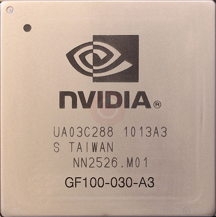
The GeForce GTX 465 was a performance-segment graphics card by NVIDIA, launched on May 31st, 2010. Built on the 40 nm process, and based on the GF100 graphics processor, in its GF100-030-A3 variant, the card supports DirectX 12. Even though it supports DirectX 12, the feature level is only 11_0, which can be problematic with newer DirectX 12 titles. The GF100 graphics processor is a large chip with a die area of 529 mm² and 3,100 million transistors. Unlike the fully unlocked GeForce GTX 480 Core 512, which uses the same GPU but has all 512 shaders enabled, NVIDIA has disabled some shading units on the GeForce GTX 465 to reach the product's target shader count. It features 352 shading units, 44 texture mapping units, and 32 ROPs. NVIDIA has paired 1,024 MB GDDR5 memory with the GeForce GTX 465, which are connected using a 256-bit memory interface. The GPU is operating at a frequency of 608 MHz, memory is running at 802 MHz (3.2 Gbps effective).
Being a dual-slot card, the NVIDIA GeForce GTX 465 draws power from 2x 6-pin power connectors, with power draw rated at 200 W maximum. Display outputs include: 2x DVI, 1x mini-HDMI 1.3a. GeForce GTX 465 is connected to the rest of the system using a PCI-Express 2.0 x16 interface. The card measures 241 mm in length, and features a dual-slot cooling solution. Its price at launch was 279 US Dollars.
Being a dual-slot card, the NVIDIA GeForce GTX 465 draws power from 2x 6-pin power connectors, with power draw rated at 200 W maximum. Display outputs include: 2x DVI, 1x mini-HDMI 1.3a. GeForce GTX 465 is connected to the rest of the system using a PCI-Express 2.0 x16 interface. The card measures 241 mm in length, and features a dual-slot cooling solution. Its price at launch was 279 US Dollars.
Graphics Processor
Graphics Card
- Release Date
- May 31st, 2010
- Generation
- GeForce 400
- Predecessor
- GeForce 200
- Successor
- GeForce 500
- Production
- End-of-life
- Launch Price
- 279 USD
- Bus Interface
- PCIe 2.0 x16
- Reviews
- 37 in our database
Relative Performance
Based on TPU review data: "Performance Summary" at 1920x1080, 4K for 2080 Ti and faster.
Clock Speeds
- GPU Clock
- 608 MHz
- Shader Clock
- 1215 MHz
- Memory Clock
-
802 MHz
3.2 Gbps effective
Memory
- Memory Size
- 1024 MB
- Memory Type
- GDDR5
- Memory Bus
- 256 bit
- Bandwidth
- 102.7 GB/s
Render Config
- Shading Units
- 352
- TMUs
- 44
- ROPs
- 32
- SM Count
- 11
- L1 Cache
- 64 KB (per SM)
- L2 Cache
- 512 KB
Theoretical Performance
- Pixel Rate
- 13.38 GPixel/s
- Texture Rate
- 26.75 GTexel/s
- FP32 (float)
- 855.4 GFLOPS
- FP64 (double)
- 106.9 GFLOPS (1:8)
Board Design
- Slot Width
- Dual-slot
- Length
- 241 mm
9.5 inches
- TDP
- 200 W
- Suggested PSU
- 550 W
- Outputs
- 2x DVI
1x mini-HDMI 1.3a
- Power Connectors
- 2x 6-pin
- Board Number
- P1025 SKU 0008
Graphics Features
- DirectX
- 12 (11_0)
- OpenGL
- 4.6
- OpenCL
- 1.1
- Vulkan
- N/A
- CUDA
- 2.0
- Shader Model
- 5.1
GF100 GPU Notes
| PureVideo HD: VP4 VDPAU: Feature Set C GF100 has 4 GPCs each capable of 8 pixels per clock. This limits complete GPU to 32 pixels per clock and because of that it can't feed all 48 ROPs when they all require data at the same time. Additional ROPs however can be used for MSAA (because it doesn't require additional data from rasterizers, while giving more work to ROPs.) |
Retail boards based on this design (3)
| Name | GPU Clock | Memory Clock | Other Changes |
|---|---|---|---|
| 608 MHz | 802 MHz | 2x DVI 1x HDMI 1x DisplayPort | |
| 608 MHz | 802 MHz | 243 mm/9.6 inches | |
| 608 MHz | 802 MHz |


May 21st, 2024 11:45 EDT
change timezone
Latest GPU Drivers
New Forum Posts
- Folding Pie and Milestones!! (9033)
- Free Download Manager output the wrong format (3)
- MSI RX 580 Armor 8GB VBios (4)
- Asus 7 PIN fans to standard 4 pin PWM? (14)
- Ryzen 5 5600x stock overclocked reaching high temps (22)
- Dell 5400 TPL Help (10)
- Fractal define R4 vs R5 build quality. (21)
- What are you playing? (20727)
- Battery swap for cyberpower UPS (93)
- Gigabyte am5 motherboard ddr5 not posting when rebooting (6)
Popular Reviews
- Ghost of Tsushima Performance Benchmark Review - 35 GPUs Tested
- Ghost of Tsushima: DLSS vs. FSR vs. XeSS Comparison Review
- PNY XLR8 Gaming EPIC-X RGB DDR5-6400 CL32 32 GB Review
- TerraMaster D8 Hybrid Review
- Silverstone Shark Force 120 mm Fan Review
- Homeworld 3 Performance Benchmark Review - 35 GPUs Tested
- Upcoming Hardware Launches 2023 (Updated Feb 2024)
- Lofree Edge Ultra-Low Profile Wireless Mechanical Keyboard Review
- AMD Ryzen 7 7800X3D Review - The Best Gaming CPU
- AMD Ryzen 7 7700 Review - Affordable Zen 4 Powerhouse
Controversial News Posts
- Intel Statement on Stability Issues: "Motherboard Makers to Blame" (269)
- AMD to Redesign Ray Tracing Hardware on RDNA 4 (227)
- Windows 11 Now Officially Adware as Microsoft Embeds Ads in the Start Menu (173)
- NVIDIA to Only Launch the Flagship GeForce RTX 5090 in 2024, Rest of the Series in 2025 (154)
- AMD Hits Highest-Ever x86 CPU Market Share in Q1 2024 Across Desktop and Server (140)
- AMD RDNA 5 a "Clean Sheet" Graphics Architecture, RDNA 4 Merely Corrects a Bug Over RDNA 3 (139)
- AMD's RDNA 4 GPUs Could Stick with 18 Gbps GDDR6 Memory (114)
- AMD Ryzen 9 7900X3D Now at a Mouth-watering $329 (104)