News Posts matching #4 nm

Return to Keyword Browsing

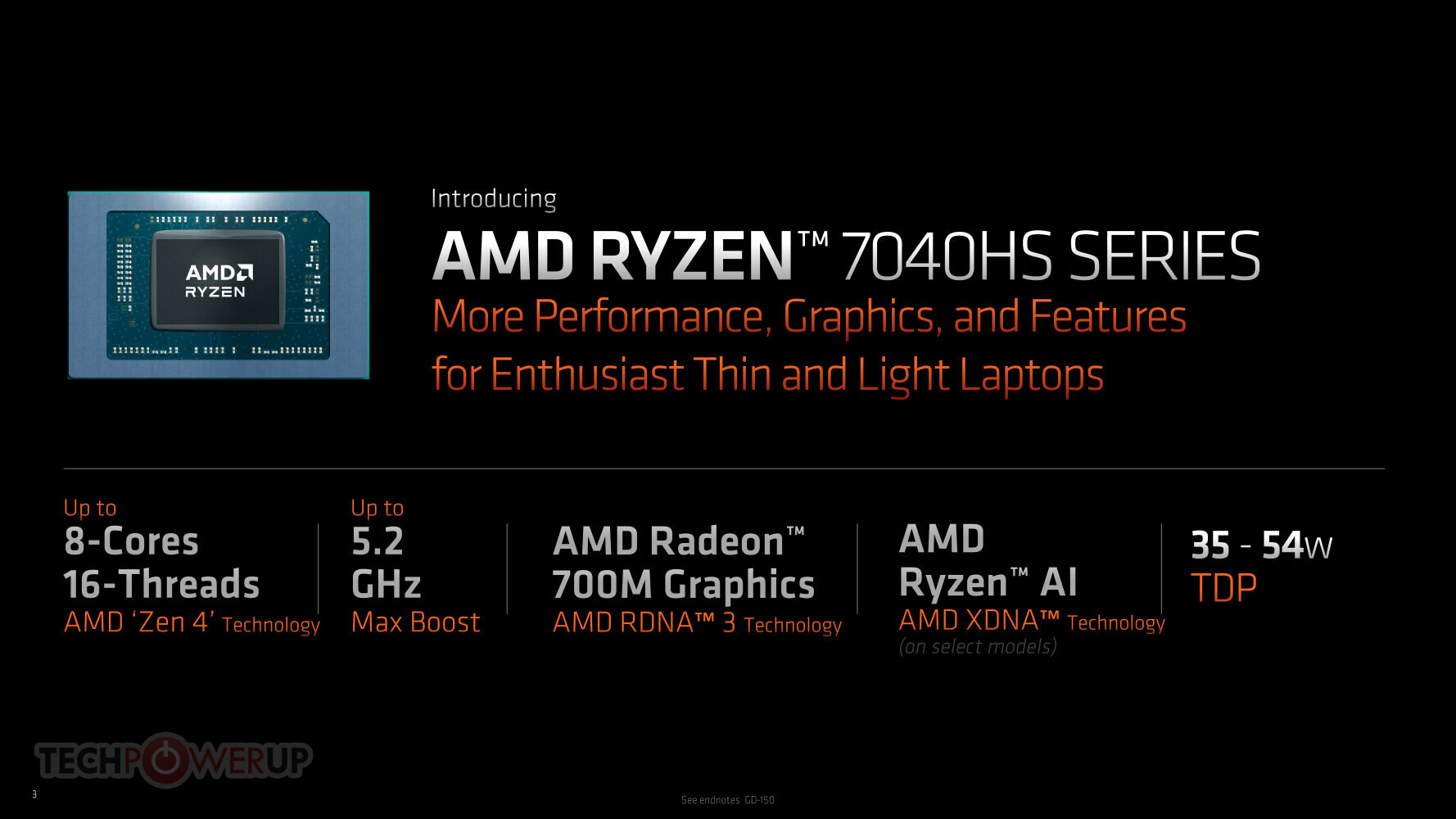
AMD Ryzen 8000G Socket AM5 Desktop APU Lineup Detailed

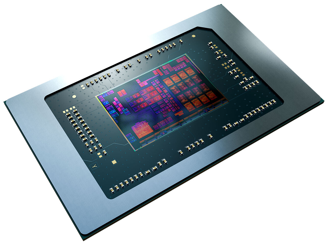
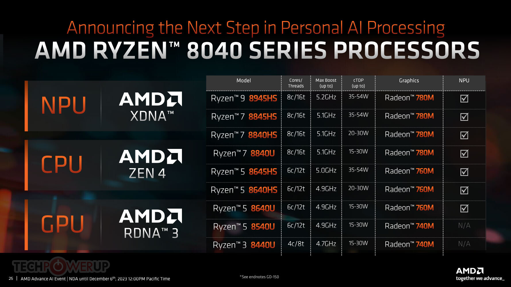
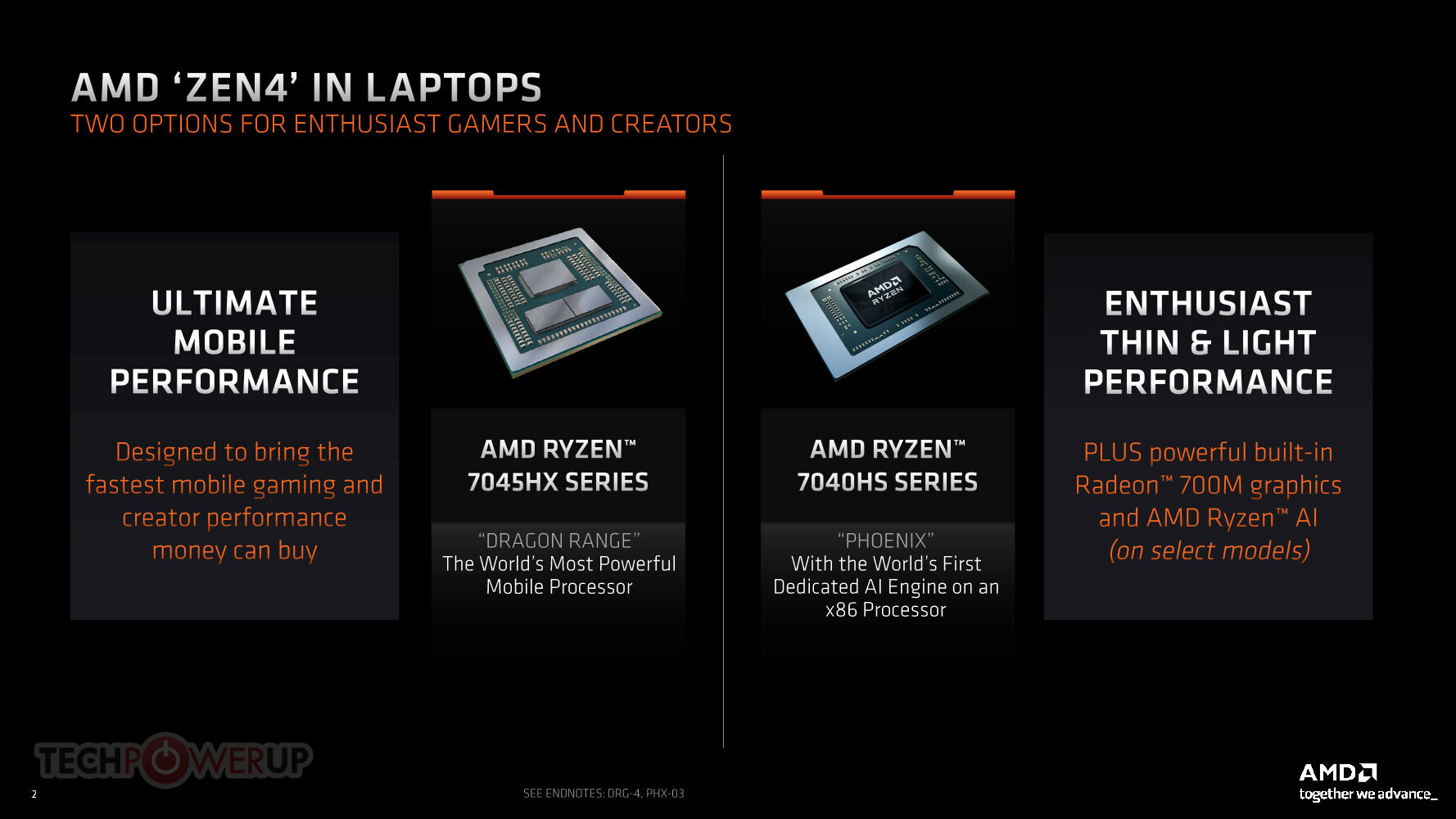
Here is our first look at the higher end of AMD's Ryzen 8000G series Socket AM5 desktop APU lineup. The company is planning to bring its 4 nm "Phoenix" and "Phoenix 2" monolithic silicon to the socketed desktop platform, to cover two distinct markets. Models based on the larger "Phoenix" silicon cater to the market that wants a sufficiently powerful CPU, but with a powerful iGPU that's fit for entry-level gaming, or graphics-intensive productivity tasks; whereas the smaller "Phoenix 2" silicon ties up the lower end of AMD's AM5 desktop processor stack, as it probably has a lower bill of materials than a "Raphael" multi-chip module.

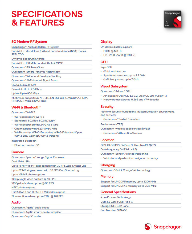
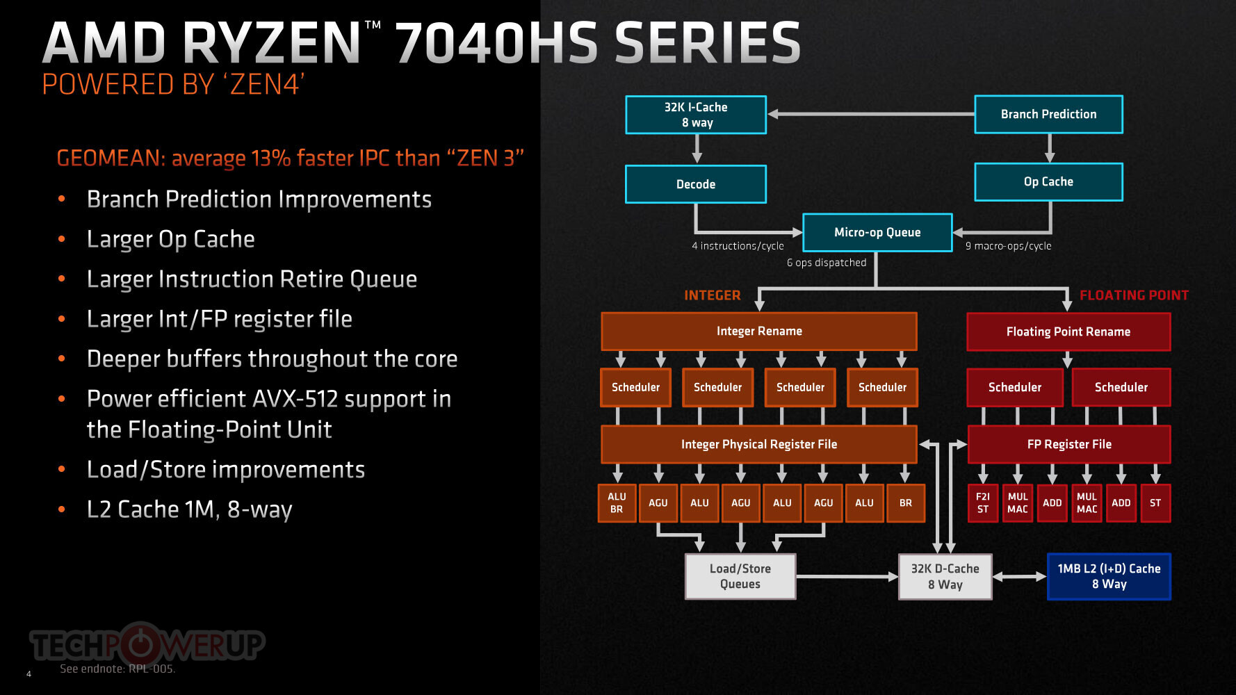
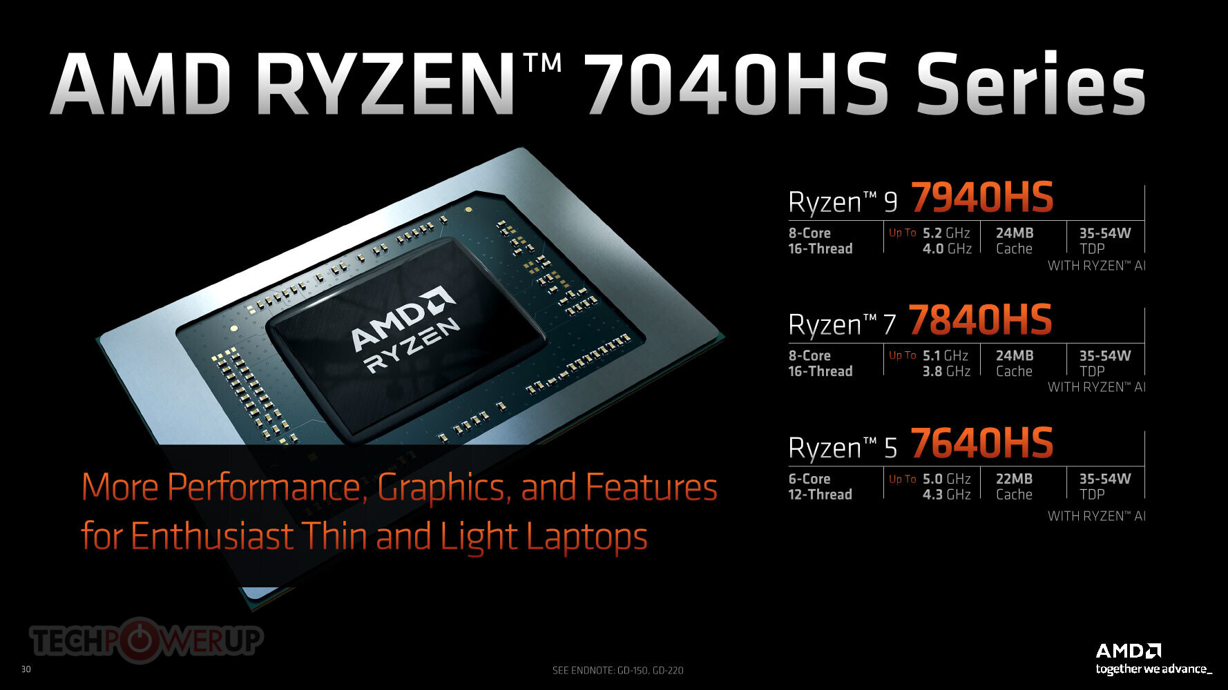
The lineup is led by the Ryzen 7 8700G, a direct successor to the Ryzen 7 5700G "Cezanne." This chip gets the full 8-core/16-thread "Zen 4" CPU, along with its 16 MB shared L3 cache; and the full featured Radeon 780M iGPU with its 12 compute units worth 768 stream processors. The CPU features a maximum boost frequency of 4.20 GHz. This is followed by the Ryzen 5 8600G, which is based on the same "Phoenix" silicon as the 8700G, but with 6 out of 8 "Zen 4" cores enabled, and a maximum CPU boost frequency of 4.35 GHz, and the 16 MB L3 cache left untouched. It's likely that the Radeon 780M is unchanged from the 8700G.
Update 13:59 UTC: A CPU-Z screenshot of the Ryzen 7 8700G surfaced, which confirms that it features the maxed out Radeon 780M iGPU

Sony PlayStation 5 Pro Packs an Updated RDNA3 GPU with 60 CU

Sony is developing the PlayStation 5 Pro console that targets higher refresh-rate gaming at 4K Ultra HD, or higher in-game eye-candy, given its faster hardware. Details about the console are few and far between, given its late-2024 tentative release, but by now the company would have co-developed its semi-custom SoC, so it could spend the next year extensively testing and optimizing it, before mass production in the 2-3 quarters leading up to the launch. Kepler_L2 and Tom Henderson on Twitter are fairly reliable sources for PlayStation hardware leaks, and piecing their recent posts together, VideoCardz compiled the most probable specs of the SoC at the heart of the PlayStation 5 Pro.

The semi-custom SoC powering the PlayStation 5 Pro is co-developed by Sony Computer Entertainment (SCE) and AMD; and is codenamed "Viola." The monolithic chip is built on the TSMC N4P foundry node (4 nm EUV), which is a big upgrade from the 7 nm DUV node on which the "Oberon" SoC powering the original PlayStation 5, and 6 nm DUV node powering the "Oberon Plus" SoC of the refreshed PS5, are based on. Sony is leaving the CPU component largely untouched, it is an 8-core/16-thread unit based on the "Zen 2" microarchitecture, spread across two 4-core CCXs. The CPU has a maximum boost frequency of 4.40 GHz, dialed up from the 3.50 GHz maximum boost of "Oberon." The iGPU is where all the magic happens.

AMD Ryzen 8040 Series "Hawk Point" Mobile Processors Announced with a Faster NPU

AMD today announced the new Ryzen 8040 mobile processor series codenamed "Hawk Point." These chips are shipping to notebook manufacturers now, and the first notebooks powered by these should be available to consumers in Q1-2024. At the heart of this processor is a significantly faster neural processing unit (NPU), designed to accelerate AI applications that will become relevant next year, as Microsoft prepares to launch Windows 12, and software vendors make greater use of generative AI in consumer applications.

The Ryzen 8040 "Hawk Point" processor is almost identical in design and features to the Ryzen 7040 "Phoenix," except for a faster Ryzen AI NPU. While this is based on the same first-generation XDNA architecture, its NPU performance has been increased to 16 TOPS, compared to 10 TOPS of the NPU on the "Phoenix" silicon. AMD is taking a whole-of-silicon approach to AI acceleration, which includes not just the NPU, but also the "Zen 4" CPU cores that support the AVX-512 VNNI instruction set that's relevant to AI; and the iGPU based on the RDNA 3 graphics architecture, with each of its compute unit featuring two AI accelerators, components that make the SIMD cores crunch matrix math. The whole-of-silicon performance figures for "Phoenix" is 33 TOPS; while "Hawk Point" boasts of 39 TOPS. In benchmarks by AMD, "Hawk Point" is shown delivering a 40% improvement in vision models, and Llama 2, over the Ryzen 7040 "Phoenix" series.

AMD Phoenix AM5 APUs to Get Ryzen 8000 Series Branding, Company Readies 5000GT Series for AM4

AMD is giving final touches to its first APUs for the Socket AM5 desktop platform. A report by Sakhtafzar Magazine suggests that the company could give processor models in the series Ryzen 8000G numbering, instead of the previously thought 7000G series. The company is preparing as many as 14 processor models spanning the 4 nm "Phoenix" and "Phoenix 2" monolithic dies. Both chips combine "Zen 4" CPU cores with an iGPU based on the RDNA 3 graphics architecture. While the current Ryzen 7000 series "Raphael" desktop processors feature integrated graphics, AMD doesn't consider them APUs, as their iGPU are just about enough for non-gaming desktop use cases. APUs are designed for entry-level gaming.

The "Phoenix" silicon has up to 8 "Zen 4" CPU cores, and an iGPU with up to 12 RDNA3 compute units. This chip is powering the Ryzen 5 8600G, Ryzen 7 8700G, their PRO variants, and their respective "GE" (energy efficient) sub-variants. The "Phoenix 2" silicon barely qualifies as an APU, as its iGPU only has 4 RDNA3 compute units (compared to the 2 RDNA2 CUs on the "Raphael" iGPU. It also has a maximum CPU core count of 6, from which two are "Zen 4" cores that can sustain higher boost frequency bins, and four are "Zen 4c" cores which run at lower clock speeds (albeit with an identical IPC and ISA). AMD is using "Phoenix 2" on the desktop platform to carve out several sub-$150 class processor models across the Ryzen 5 and Ryzen 3 brands; a package with a monolithic "Phoenix 2" die probably has a lower bill of materials (BOM) than a "Raphael" multi-chip module.

MediaTek's New Dimensity 8300 Chipset Redefines Premium Experiences in 5G Smartphones

MediaTek today announced the Dimensity 8300, a power-efficient chipset designed for premium 5G smartphones. As the newest SoC in the Dimensity 8000 lineup, this chipset combines generative AI capabilities, low-power savings, adaptive gaming technology, and fast connectivity to bring flagship-level experiences to the premium 5G smartphone segment.

Based on TSMC's 2nd generation 4 nm process, the Dimensity 8300 has an octa-core CPU with four Arm Cortex-A715 cores and four Cortex-A510 cores built on Arm's latest v9 CPU architecture. With this powerful core configuration, the Dimensity 8300 boasts 20% faster CPU performance and 30% peak gains in power efficiency compared to the previous generation chipset. Additionally, the Dimensity 8300's Mali-G615 MC6 GPU upgrade provides up to 60% greater performance and 55% better power efficiency. Plus, the chipset's impressive memory and storage speeds ensure users can enjoy smooth and dynamic experiences in gaming, lifestyle applications, photography, and more.

AMD Readies Even More Derivatives of the 4 nm "Phoenix" Processor Silicon

AMD's "Phoenix" monolithic processor silicon drives the company's Ryzen 7040 series mobile processor lineup, and possible some of its upcoming Ryzen 7000G desktop processor models. It is the first chip from the AMD camp to feature an AI accelerator, besides up to 8 "Zen 4" CPU cores, and a large iGPU based on the latest RDNA3 graphics architecture, with up to 12 compute units, the latest display I/O and media acceleration capabilities. Over the course of its lifecycle, AMD realized that it can't use the nearly 200 mm² silicon built on the expensive 4 nm node to power lower-end processor SKUs, and so developed the smaller 137 mm² "Phoenix 2" silicon that lacks the AI accelerator, has a smaller iGPU with just 4 compute units, and a unique hybrid CPU with 2 "Zen 4" and 4 "Zen 4c" cores. We're now hearing that the company is designing even more derivatives.

The PCI ID Repository discovered two new IDs believed to reference the iGPU models of "Phoenix 3" and "Phoenix 4" chips. At this point we have no clue what the two chips could be, and what the mixture of their CPU, iGPU, and AI accelerator components could be, especially given that AMD is able to carve out Ryzen 3 SKUs from "Phoenix 2." We speculate that "Phoenix 3" and "Phoenix 4" could reference rebranding such as "Escher," although it could even be entirely new chips with different combinations of "Zen 4" and "Zen 4c" cores.

Ventana Introduces Veyron V2 - World's Highest Performance Data Center-Class RISC-V Processor and Platform

Ventana Micro Systems Inc. today announced the second generation of its Veyron family of RISC-V processors. The new Veyron V2 is the highest performance RISC-V processor available today and is offered in the form of chiplets and IP. Ventana Founder and CEO Balaji Baktha will share the details of Veyron V2 today during his keynote speech at the RISC-V Summit North America 2023 in Santa Clara, California.

"Veyron V2 represents a leap forward in our quest to lead the industry in high-performance RISC-V CPUs that are ready for rapid customer adoption," said Balaji Baktha, Founder and CEO of Ventana. "It substantiates our commitment to customer innovation, workload acceleration, and overall optimization to achieve best in class performance per Watt per dollar. V2 enhancements unleash innovation across data center, automotive, 5G, AI, and client applications."

MediaTek Announces the Dimensity 9300 Flagship SoC, with Big Cores Only

MediaTek today announced the Dimensity 9300, its newest flagship mobile chip with a one-of-a-kind All Big Core design. The unique configuration combines extreme performance with MediaTek's industry-leading power efficiency to deliver unmatched user experiences in gaming, video capture and on-device generative AI processing.

"The Dimensity 9300 is MediaTek's most powerful flagship chip yet, bringing a huge boost in raw computing power to flagship smartphones with our groundbreaking All Big Core design," said Joe Chen, President at MediaTek. "This unique architecture, combined with our upgraded on-chip AI Processing Unit, will usher in a new era of generative AI applications as developers push the limits with edge AI and hybrid AI computing capabilities."

AMD Introduces Ryzen 5 and Ryzen 3 Mobile Processors with "Zen 4c" Cores

AMD today launched its first client processors that feature the compact "Zen 4c" CPU cores, with the Ryzen 5 7545U and Ryzen 3 7440U mobile processors for thin-and-light notebooks. The "Zen 4c" CPU core is a compacted version of the "Zen 4" core without the subtraction of any hardware components, but rather a high density arrangement of them on the 4 nm silicon. A "Zen 4c" core is around 35% smaller in area on the die than a regular "Zen 4" core. Since none of its components is removed, the core features an identical IPC (single thread performance) to "Zen 4," as well as an identical ISA (instruction set). "Zen 4c" also supports SMT or 2 threads per core. The trade-off here is that "Zen 4c" cores are generally clocked lower than "Zen 4" cores, as they can operate at lower core voltages. This doesn't, however, make the "Zen 4c" comparable to an E-core by Intel's definition, these cores are still part of the same CPU clock speed band as the "Zen 4" cores, at least in the processors that's being launched today.

The Ryzen 5 7545U and Ryzen 3 7440U mobile processors formally debut the new 4 nm "Phoenix 2" monolithic silicon. This chip is AMD's first hybrid processor, in that it has a mixture of two regular "Zen 4" cores, and four compact "Zen 4c" cores. The six cores share an impressive 16 MB of L3 cache. All six cores feature 1 MB of dedicated L2 cache. There is no complex hardware-based scheduler involved, but a software based solution that's deployed by AMD's Chipset Software, which tells the Windows scheduler to see the "Zen 4" cores as UEFI CPPC "preferred cores," and prioritize traffic to them, as they can hold on to higher boost frequency bins. The "Phoenix 2" silicon inherits much of the on-die power-management feature-set from the "Phoenix" and "Rembrandt" chips, and so are capable of a high degree of power savings with underutilized CPU cores and iGPU compute units.

AMD Mobile Processor Lineup in 2025 Sees "Fire Range," "Strix Halo," and Signficant AI Performance Increases

With Windows 11 23H2 setting the stage for increased prevalence of AI in client PC use cases, the new hardware battleground between AMD and its rivals Intel, Apple, and Qualcomm, will be in equipping their mobile processors with sufficient AI acceleration performance. AMD already introduced accelerated AI with the current "Phoenix" processor that debuts Ryzen AI, and its Xilinx XDNA hardware backend that provides a performance of up to 16 TOPS. This will see a 2-3 fold increase with the company's 2024-25 mobile processor lineup, according to a roadmap leak by "Moore's Law is Dead."

At the very top of the pile, in a product segment called "ultimate compute," which consists of large gaming notebooks, mobile workstations, and desktop-replacements; the company's current Ryzen 7045 "Dragon Range" processor will continue throughout 2024. Essentially a non-socketed version of the desktop "Raphael" MCM, "Dragon Range" features up to two 5 nm "Zen 4" CCDs for up to 16 cores, and a 6 nm cIOD. This processor lacks any form of AI acceleration. In 2025, the processor will be succeeded with "Fire Range," a similar non-socketed, mobile-friendly MCM that's derived from "Granite Ridge," with up to two 4 nm "Zen 5" CCDs for up to 16 cores; and the 6 nm cIOD. What's interesting to note here, is that the quasi-roadmap makes no mention of AI acceleration for "Fire Range," which means "Granite Ridge" could miss out on Ryzen AI acceleration from the processor. Modern discrete GPUs from both NVIDIA and AMD support AI accelerators, so this must have been AMD's consideration to exclude an XDNA-based Ryzen AI accelerator on "Fire Range" and "Granite Ridge."

Samsung Electronics Announces Third Quarter 2023 Results

Samsung Electronics today reported financial results for the third quarter ended September 30, 2023. Total consolidated revenue was KRW 67.40 trillion, a 12% increase from the previous quarter, mainly due to new smartphone releases and higher sales of premium display products. Operating profit rose sequentially to KRW 2.43 trillion based on strong sales of flagship models in mobile and strong demand for displays, as losses at the Device Solutions (DS) Division narrowed.

The Memory Business reduced losses sequentially as sales of high valued-added products and average selling prices somewhat increased. Earnings in system semiconductors were impacted by a delay in demand recovery for major applications, but the Foundry Business posted a new quarterly high for new backlog from design wins. The mobile panel business reported a significant increase in earnings on the back of new flagship model releases by major customers, while the large panel business narrowed losses in the quarter. The Device eXperience (DX) Division achieved solid results due to robust sales of premium smartphones and TVs. Revenue at the Networks Business declined in major overseas markets as mobile operators scaled back investments.

Qualcomm Snapdragon Elite X SoC for Laptop Leaks: 12 Cores, LPDDR5X Memory, and WiFi7

Thanks to the information from Windows Report, we have received numerous details regarding Qualcomm's upcoming Snapdragon Elite X chip for laptops. The Snapdragon Elite X SoC is built on top of Nuvia-derived Oryon cores, which Qualcomm put 12 off in the SoC. While we don't know their base frequencies, the all-core boost reaches 3.8 GHz. The SoC can reach up to 4.3 GHz on single and dual-core boosting. However, the slide notes that this is all pure "big" core configuration of the SoC, so no big.LITTLE design is done. The GPU part of Snapdragon Elite X is still based on Qualcomm's Adreno IP; however, the performance figures are up significantly to reach 4.6 TeraFLOPS of supposedly FP32 single-precision power. Accompanying the CPU and GPU, there are dedicated AI and image processing accelerators, like Hexagon Neural Processing Unit (NPU), which can process 45 trillion operations per second (TOPS). For the camera, the Spectra Image Sensor Processor (ISP) is there to support up to 4K HDR video capture on a dual 36 MP or a single 64 MP camera setup.

The SoC supports LPDDR5X memory running at 8533 MT/s and a maximum capacity of 64 GB. Apparently, the memory controller is an 8-channel one with a 16-bit width and a maximum bandwidth of 136 GB/s. Snapdragon Elite X has PCIe 4.0 and supports UFS 4.0 for outside connection. All of this is packed on a die manufactured by TSMC on a 4 nm node. In addition to marketing excellent performance compared to x86 solutions, Qualcomm also advertises the SoC as power efficient. The slide notes that it uses 1/3 of the power at the same peak PC performance of x86 offerings. It is also interesting to note that the package will support WiFi7 and Bluetooth 5.4. Officially coming in 2024, the Snapdragon Elite X will have to compete with Intel's Meteor Lake and/or Arrow Lake, in addition to AMD Strix Point.

Latest AMD AGESA Hints at Ryzen 7000G "Phoenix" Desktop APUs

AMD is preparing to launch its first APUs on the Socket AM5 desktop platform, with the Ryzen 7000G series. While the company has standardized integrated graphics with the Ryzen 7000 series, it does not consider the regular Ryzen 7000 series "Raphael" processors as APUs. AMD considers APUs to be processors with overpowered iGPUs that are fit for entry-mainstream PC gaming. As was expected for a while now, for the Ryzen 7000G series, AMD is tapping into its 4 nm "Phoenix" monolithic silicon, the same chip that powers the Ryzen 7040 series mobile processors. Proof of "Phoenix" making its way to desktop surfaced with CPU support lists for the latest AGESA SMUs (system management units) compiled by Reous, with the AGESA ComboAM5PI 1.0.8.0 listing support for "Raphael," as well as "Phoenix." Another piece of evidence was an ASUS B650 motherboard support page that listed a UEFI firmware update encapsulating 1.0.8.0, which references an "upcoming CPU."

Unlike "Raphael" and "Dragon Range," "Phoenix" is a monolithic processor die built on the TSMC 4 nm foundry node. Its CPU is based on the latest "Zen 4" microarchitecture, and features an 8-core/16-thread configuration, with 1 MB of L2 cache per core, and 16 MB of shared L3 cache. The star attraction here is the iGPU, which is based on the RDNA3 graphics architecture, meets the DirectX 12 Ultimate feature requirements, and is powered by 12 compute units worth 768 stream processors. Unlike "Raphael," the "Phoenix" silicon is known to feature an older PCI-Express Gen 4 root complex, with 24 lanes, so you get a PCI-Express 4.0 x16 PEG slot, one CPU-attached M.2 NVMe slot limited to Gen 4 x4, and a 4-lane chipset bus. "Phoenix" features a dual-channel (4 sub-channel) DDR5 memory controller, with native support for DDR5-5600. A big unknown with the Ryzen 7000G desktop APUs is whether they retain the Ryzen AI feature-set from the Ryzen 7040 series mobile processors.

Tenstorrent Selects Samsung Foundry to Manufacture Next-Generation AI Chiplet

Tenstorrent, a company that sells AI processors and licenses AI and RISC-V IP, announced today that it selected Samsung Foundry to bring Tenstorrent's next generation of AI chiplets to market. Tenstorrent builds powerful RISC-V CPU and AI acceleration chiplets, aiming to push the boundaries of compute in multiple industries such as data center, automotive and robotics. These chiplets are designed to deliver scalable power from milliwatts to megawatts, catering to a wide range of applications from edge devices to data centers.

To ensure the highest quality and cutting-edge manufacturing capabilities for its chiplet, Tenstorrent has selected Samsung's Foundry Design Service team, known for their expertise in silicon manufacturing. The chiplets will be manufactured using Samsung's state-of-the-art SF4X process, which boasts an impressive 4 nm architecture.

More AMD "Strix Point" Mobile Processor Details Emerge

"Strix Point" is the codename for AMD's next-generation mobile processor succeeding the current Ryzen 7040 series "Phoenix." More details of the processor emerged thanks to "All The Watts!!" on Twitter. The CPU of "Strix Point" will be heterogenous, in that it will feature two different kinds of CPU cores, but with essentially the same ISA and IPC. It is rumored that the processor will feature 4 "Zen 5" CPU cores, and 8 "Zen 5c" cores.

Both core types feature an identical IPC, but the "Zen 5" cores can hold onto higher boost frequencies, and have a wider frequency band, than the "Zen 5c" cores. From what we can deduce from the current "Zen 4c" cores, "Zen 5c" cores aren't strictly "efficiency" cores, as they still offer the full breadth of core ISA as "Zen 5," including SMT. In its maximum configuration, "Strix Point" will hence be a 12-core/24-thread processor. The two CPU core types sit in two different CCX (CPU core complexes), the "Zen 5" CCX has 4 cores sharing a 16 MB L3 cache, while the "Zen 5c" CCX shares a 16 MB L3 cache among 8 cores. AMD will probably use a software-based solution to ensure the right kind of workload from the OS is processed by the right kind of CPU core.

Top Ten Semiconductor Foundries Report a 1.1% Quarterly Revenue Decline in 2Q23, Anticipated to Rebound in 3Q23

TrendForce reports an interesting shift in the electronics landscape: dwindling inventories for TV components, along with a surging mobile repair market that's been driving TDDI demand, have sparked a smattering of urgent orders in the Q2 supply chain. These last-minute orders have served as pivotal lifelines, propping up Q2 capacity utilization and revenue for semiconductor foundries. However, the adrenaline rush from these stop-gap orders may be a short-lived phenomenon and is unlikely to be carried over into the third quarter.

On the other hand, demand for staple consumer products like smartphones, PCs, and notebooks remains sluggish, perpetuating a slump in the use of expensive, cutting-edge manufacturing processes. At the same time, traditionally stable sectors—automotive, industrial control, and servers—are undergoing inventory correction. The confluence of these trends has resulted in a sustained contraction for the world's top ten semiconductor foundries. Their global revenue declined by approximately 1.1% for the quarter, amounting to a staggering US$26.2 billion.

Samsung Claims Higher 3 nm Yields than TSMC

Competition between Samsung and TSMC in the 4 nm and 3 nm foundry process markets is about to heat up, with the Korean foundry claiming yields competitive to those of TSMC, according to a report in the Kukmin Ilbo, a Korean daily newspaper. 4 nm is the final silicon fabrication process to use the FinFET technology that powered nodes ranging between 16 nm to 4 nm. Samsung Foundry is claiming 4 nm wafer yields of 75%, against the 80% yields figure put out by TSMC. 4 nm powers several current-generation mobile SoCs, PC processors, and more importantly, the GPUs driving the AI gold-rush.

Things get very interesting with 3 nm, the node that debuts GAA-FET (gates all around FET) technology. Here, Samsung claims to offer higher yields than TSMC, with its 3 nm GAA node clocking 60% yields, against 55% put out by TSMC. Samsung was recently bitten by a scandal where its engineers allegedly falsified yields figures to customers to score orders, which had a cascading effect on the volumes and competitiveness of their customers. We're inclined to think that Samsung has taken lessons and is more careful with the yields figures being reported in the press. Meanwhile, Intel Foundry Services competes with the Intel 3 node, which is physically 7 nm FinFET, but with electrical characteristics comparable to those of 3 nm.

AMD Ryzen 7040H Series Exclusive to China, 7040HS Assigned to Regions Outside of PRC

AMD's laptop-oriented Ryzen 7040 series of Zen 4 processors APUs—based on 4 nm "Phoenix" monolithic silicon—have been slow to hit the market, but folks have had plenty of time to study spec sheets and press material. The presence of similar-ish 7040HS and 7040H product assignments (also sharing nearly identical specifications) has caused some confusion within the PC hardware community. Team Red has finally got round to explaining the significance of their -HS and -H identifiers—product pages were updated with new information this month, showing that the Ryzen 7040H series exists as a Chinese market exclusive. NA, EMEA, APJ, LATAM regions will be getting the closely related Ryzen 7040HS lineup instead. ASUS, Lenovo, and Machenike are set to launch new laptop models in China that will feature Ryzen 7040H APUs—VideoCardz found it interesting that "some of them will not have discrete graphics and will have a higher TDP of 65 W".

AMD Ryzen 5 7500F Desktop Processor Surfaces, Could this be Phoenix-2 on AM5?

A screenshot from Puget Systems benchmark database reveals a new upcoming desktop processor model by AMD, the Ryzen 5 7500F. The screenshot details the 7500F as a 6-core processor, and the machine features an ASUS ROG Strix X670E-F Gaming motherboard, along with an RTX 4080 graphics card. At this point it's hard to tell what the "F" brand extension means in AMD nomenclature. On Intel, it denotes a lack of integrated graphics.

There are two possible theories on what the 7500F could be. One holds that it's a down-rated "Raphael" MCM with a disabled iGPU; while the other holds that it could be based on the 4 nm Phoenix-2 monolithic silicon. Detailed in an older article, the Phoenix-2 is a 137 mm² monolithic silicon that physically features no more than 6 "Zen 4" CPU cores, and an iGPU with just 4 RDNA 3 compute units, besides I/O that's identical to that of the regular 178 mm² 8-core/12-CU Phoenix silicon. Phoenix-2 on AM5 might just end up with a lower bill of materials than a single-CCD "Raphael" MCM.

Update 06:13 UTC: A Korean retailer has posted the first picture of the Ryzen 5 7500F in the flesh. They claim a street price of around $170-180 (KRW equivalent), and availability slated for July 7.

AMD Designs Physically Smaller "Phoenix 2" Die with 6-core CPU and 4 CU iGPU

AMD has designed a physically smaller version of its 4 nm "Phoenix" mobile processor silicon. The chip could power lower-end mobile SKUs in the Ryzen 3 and Ryzen 5 series, and it's likely that it could make it to Socket AM5, where it will power Ryzen 3 and lower-end versions of Ryzen 5 desktop processors. Built on the same 4 nm foundry process as the standard "Phoenix" silicon, the so-called "Phoenix 2" or "PHX2" die physically features a 6-core/12-thread CPU based on the "Zen 4" microarchitecture, and a physically smaller iGPU with just two WGPs (workgroup processors), or 4 CU (compute units), which work out to 256 stream processors. This iGPU is based on the same RDNA3 graphics architecture as the one powering the regular "Phoenix" silicon. At this point we don't know if the Ryzen AI component gets the axe, but given AMD's enthusiasm with consumer AI acceleration, the die might just retain it.

The PHX2 die likely retains the I/O of the regular "Phoenix," including a dual-channel (4 sub-channel) DDR5 and LPDDR5 memory interface, and a 24-lane PCI-Express Gen 4 root complex. These changes result in a die that appears to be around three-quarters the size of the regular "Phoenix," with an area of around 137 mm², compared to 178 mm² of the regular "Phoenix." The smaller die will save AMD big on costs and yields. At this time, there are at least two processor models reported to be based on this die, the Ryzen 5 7540U and Ryzen 3 7440U. Both are 15 W to 28 W class mobile processors aimed at thin-and-light notebooks.

Qualcomm Introduces Value Oriented Snapdragon 4 Gen 2 Mobile Platform

Qualcomm Technologies, Inc. has announced the new Snapdragon 4 Gen 2 Mobile Platform, which has been creatively engineered to make incredible mobile experiences accessible to more consumers globally. Snapdragon 4 Gen 2 provides effortless, all-day use with fast CPU speeds, sharp photography and videography, plus speedy 5G and Wi-Fi for reliable connections.

"Snapdragon - at its core - is driving innovation while meeting the demands of OEMs and the broader industry," said Matthew Lopatka, director of product management, Qualcomm Technologies, Inc. "With this generational advancement in the Snapdragon 4-series, consumers will have greater access to the most popular and relevant mobile features and capabilities. We optimized every aspect of the platform in order to maximize the experiences for users."

Samsung Electronics Unveils Foundry Vision in the AI Era

Samsung Electronics, a world leader in advanced semiconductor technology, today announced its latest foundry technology innovations and business strategy at the 7th annual Samsung Foundry Forum (SFF) 2023. Under the theme "Innovation Beyond Boundaries," this year's forum delved into Samsung Foundry's mission to address customer needs in the artificial intelligence (AI) era through advanced semiconductor technology.

Over 700 guests, from customers and partners of Samsung Foundry, attended this year's event, of which 38 companies hosted their own booths to share the latest technology trends in the foundry industry.

AMD Announces Ryzen 7040HS "Zen 4" Processors for Notebooks

AMD today launched its Ryzen 7040HS line of mobile processors targeting consumer notebooks of conventional thickness and portability, which AMD considers thin-and-light. This class of devices is positioned between ultraportable notebooks, and gaming notebooks or portable workstations. AMD already powers several segments of gaming notebooks and portable workstations with its Ryzen 7045HX series "Dragon Range" mobile processors, with CPU core counts ranging between 6 and 16; as well as the ultraportable segment with the Ryzen 7040U series; but while the 7045 series have their TDP rated in the 45 W to 65 W range, and the Ryzen 7040U in the 15 W to 28 W range, the company was lacking a current-generation processor lineup in the 35 W to 54 W segment, which the company is filling up with today's Ryzen 7040HS series launch.

The Ryzen 7040HS series processors are based on the 4 nm "Phoenix" monolithic silicon, just like the 7040U series, and is based on a combination of "Zen 4" microarchitecture for its CPU, RDNA3 graphics architecture for its iGPU, and the new XDNA architecture for its Ryzen AI on-chip accelerator. Physically, the "Phoenix" silicon features an 8-core/16-thread "Zen 4" CPU. Each core has 1 MB of dedicated L2 cache, and a 16 MB L3 cache is shared among the 8 cores. The iGPU features 12 RDNA3 compute units, which amount to 768 stream processors, along with 24 AI Accelerators (specific to the RDNA3 architecture); 24 Ray Accelerators, 48 TMUs, and 32 ROPs. The iGPU meets the full DirectX 12 Ultimate logo requirements. The Ryzen AI XDNA accelerator features 20 AI acceleration tiles, each with local memory.

Top 10 Foundries Report Nearly 20% QoQ Revenue Decline in 1Q23, Continued Slide Expected in Q2

TrendForce reports that the global top 10 foundries witnessed a significant 18.6% QoQ decline in revenue during the first quarter of 2023. This decline—amounting to approximately US$27.3 billion—can be attributed to sustained weak end-market demand and the compounded effects of the off-peak season. The rankings also underwent notable changes, with GlobalFoundries surpassing UMC to secure the third position, and Tower Semiconductor surpassing PSMC and VIS to claim the seventh spot.

Declining capacity utilization rate and shipment volume contribute to widened revenue decline
The revenue decline in Q1 was primarily influenced by declining capacity utilization rates and shipment volume across the top 10 foundries. For instance, TSMC generated US$16.74 billion in revenue—marking a 16.2% QoQ drop in revenue. Weakened demand for mainstream applications such as laptops and smartphones led to a significant decline in the utilization rates and revenue of the 7/6 nm and 5/4 nm processes, falling over 20% and 17%, respectively. While the second quarter may see temporary relief coming from rush orders, the persistently low capacity utilization rate indicates that revenue is likely to continue declining, albeit at a slower pace compared to Q1.

AMD Confirms Zen 5 will Get Ryzen 8000 Series Branding, "Navi 3.5" Graphics in 2024

AMD in one of its Meet the Experts presentations to the retail channel vendors, confirmed that the next-generation "Zen 5" architecture will see its desktop part branded under the Ryzen 8000 series. The company has known to skip a thousand-number sequence each generation for its mainstream-desktop series, the way it skipped Ryzen 4000 series nomenclature between the "Zen 2" based Ryzen 3000 "Vermeer" and "Zen 3" based Ryzen 5000 Vermeer; and more recently, between "Vermeer" and the "Zen 4" based Ryzen 7000 "Raphael," which makes this an interesting development. AMD's next-generation mainstream-desktop processor is expected to be codenamed "Granite Ridge," it will feature up to 16 "Zen 5" CPU cores across up to two CCDs. The processor I/O (and its 6 nm cIOD) is expected to be largely carried over, except that it could be upgraded with support for higher DDR5 memory speeds.

Another major disclosure is the very first mention of "Navi 3.5" This implies an incremental to the "Navi 3.0" generation (Radeon RX 7000 series, RDNA3 graphics architecture), which could even be a series-wide die-shrink to a new foundry node such as TSMC 4 nm, or even 3 nm; which scoops up headroom to dial up clock speeds. AMD probably finds its current GPU product stack in a bit of a mess. While the "Navi 31" is able to compete with NVIDIA's high-end SKUs such as the RTX 4080, and the the company expected to release slightly faster RX 7950 series to have a shot at the RTX 4090; the company's performance-segment, and mid-range GPUs may have wildly missed their performance targets to prove competitive against NVIDIA's AD104-based RTX 4070 series, and AD106-based RTX 4060 series; with its recently announced RX 7600 being based on older 6 nm foundry tech, and performing a segment lower than the RTX 4060 Ti.
Return to Keyword Browsing
May 21st, 2024 18:29 EDT change timezone

New Forum Posts

Popular Reviews

Controversial News Posts