News Posts matching #4 nm

Return to Keyword Browsing

AMD Announces the "Zen 5" Microarchitecture and EPYC "Turin" Processor on 4nm

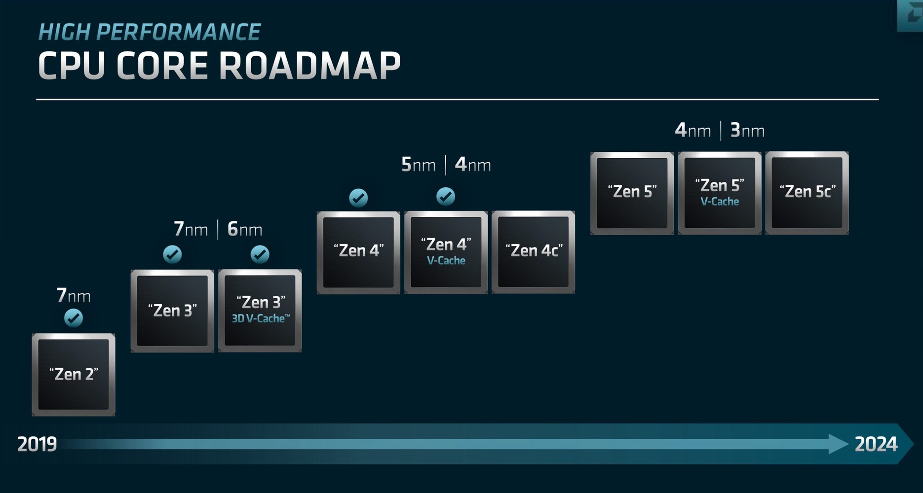
AMD in its Financial Analyst Day 2022 presentation, unveiled its next-generation "Zen 5" CPU microarchitecture. The company's latest CPU microarchitecture roadmap also confirms that variants of its "Zen 4" CCDs with 3D Vertical Cache (3DV Cache) are very much in the works, and there will be variants of the EPYC "Genoa" processors with 3DV Cache, besides standard ones.

AMD stated that it completed the design goal of the current "Zen 3" architecture, by building it on both 7 nm and 6 nm nodes (the latter being the client "Rembrandt" processor). The new "Zen 4" architecture will debut on the 5 nm node (TSMC N5), and could see a similar optical shrink to the newer 4 nm node somewhere down the line, although AMD wouldn't specify whether it's on the enterprise segment, or client. The next-gen "Zen 5" architecture will debut on 4 nm, and see an optical shrink to 3 nm on some future product.

After TSMC, Intel May be Edging Closer to Samsung for Collaboration

Intel's revamped IDM 2.0 strategy has seen the company revise its stance in both in-house and outsourced silicon fabrication. While we're already seeing the fruits of Intel's collaboration with TSMC (albeit at the relatively slow pace of introduction for Intel's Arc Alchemist graphics), it seems that Intel is willing to go much farther than just TSMC as a source of chips for its product portfolio.

That's the backdrop to which Intel CEO Pat Gelsinger recently took a trip to South Korea's capital of Seoul. According to the Korea Herald, Gelsinger met several key Samsung executives, including Samsung Electronics Vice Chairman Lee Jae-yong, co-CEO and chip business boss Kyung Kye-hyun, and head of Samsung Mobile Roh Tae-moon. More than enough executive grunt to ignite talks of a deepening collaboration between both companies. While the reporting source doesn't provide any quotes or actionable intel from the meeting, Samsung remains one of the key semiconductor manufacturers alongside Intel itself and TSMC, with a particularly strong portfolio in memory-related technologies.

Samsung Foundry Considering up to 20 Percent Price Hikes

Earlier this week, news about TSMC increasing prices in 2023 made its way online and now Samsung Foundry is said to be discussing price hikes with its customers to make up for the increased costs in materials. TSMC already increased its prices by around 20 percent at the end of 2021 and now it looks like Samsung Foundry is set to follow suit with a similar price hike. Depending on the node, the company is said to be looking at increases of between 15 to 20 percent. The somewhat peculiar thing in the case of Samsung Foundry, is that the company is looking at asking for more money on older, legacy nodes, than it will for its cutting edge nodes.

The price increases are said to come into effect sometime in the second half of 2022, so more than six months after TSMC's price hike. The company is still in negotiation with some of its customers, while others have already come to an agreement with Samsung Foundries. The costs to produce chips are said to be increasing by 20 to 30 percent across the board, no matter if we're talking materials needed to produce integrated circuits, or building new factories, according to Bloomberg. Samsung Foundries have also managed to secure long-term orders for the next five years, with a combined value of around eight times that of previous year's revenue, according to its EVP, Kang Moon-soo. The company is hoping to overtake TSMC in the future and invested more than US$36 billion in 2021 alone to expand its foundry business with new fabs and EUV machines. The good news is that Samsung Foundry claims to be back on track when it comes to yield on its 4 nm node and mass production of its 3 nm node is said to start this quarter.

NVIDIA H100 SXM Hopper GPU Pictured Up Close

ServeTheHome, a tech media outlet focused on everything server/enterprise, posted an exclusive set of photos of NVIDIA's latest H100 "Hopper" accelerator. Being the fastest GPU NVIDIA ever created, H100 is made on TSMC's 4 nm manufacturing process and features over 80 billion transistors on an 814 mm² CoWoS package designed by TSMC. Complementing the massive die, we have 80 GB of HBM3 memory that sits close to the die. Pictured below, we have an SXM5 H100 module packed with VRM and power regulation. Given that the rated TDP for this GPU is 700 Watts, power regulation is a serious concern and NVIDIA managed to keep it in check.

On the back of the card, we see one short and one longer mezzanine connector that acts as a power delivery connector, different from the previous A100 GPU layout. This board model is labeled PG520 and is very close to the official renders that NVIDIA supplied us with on launch day.

NVIDIA Hopper Whitepaper Reveals Key Specs of Monstrous Compute Processor

The NVIDIA GH100 silicon powering the next-generation NVIDIA H100 compute processor is a monstrosity on paper, with an NVIDIA whitepaper published over the weekend revealing its key specifications. NVIDIA is tapping into the most advanced silicon fabrication node currently available from TSMC to build the compute die, which is TSMC N4 (4 nm-class EUV). The H100 features a monolithic silicon surrounded by up to six on-package HBM3 stacks.

The GH100 compute die is built on the 4 nm EUV process, and has a monstrous transistor-count of 80 billion, a nearly 50% increase over the GA100. Interestingly though, at 814 mm², the die-area of the GH100 is less than that of the GA100, with its 826 mm² die built on the 7 nm DUV (TSMC N7) node, all thanks to the transistor-density gains of the 4 nm node over the 7 nm one.

Samsung Says Future Fab Nodes Are On Time, no Yield Issues on Current Nodes

Despite rumours of both production issues and node delays, Samsung has assured its shareholders during its first quarter conference call, that the company is on track. Its yield rate from its 5 nm node was said to have entered maturity, meaning that yields have entered Samsung's expected levels. However, Samsung did admit that its 4 nm node had seen some delays with the ramp up, but it has now entered the expected yield rate curve. The company is also working on an new R&D line for its upcoming 3 nm node, but didn't go into any further details.

As for Samsung's DRAM products, there were rumours that its 12 nm 1b process node had hit some snags and that the company was going to skip ahead to its 1c node, something the company denied. Samsung added that the development of 1b was proceeding stably and that the 1c node is expected to be done on schedule. The company also said that media reports of issues at Samsung's foundry business were overblown and that order books are full, which is why some of its customers have had to produce additional parts with TSMC. Samsung's foundry business reportedly saw an increase in operating profit of 50 percent compared to last year, as well as an increase in revenue of 19 percent.

TSMC Ramps up Shipments to Record Levels, 5/4 nm Production Lines at Capacity

According to DigiTimes, TSMC is working on increased its monthly shipments of finished wafers from 120,000 to 150,000 for its 5 nm nodes, under which 4 nm also falls. This is three times as much as what TSMC was producing just a year ago. The 4 nm node is said to be in full mass production now and the enhanced N4P node should be ready for mass production in the second half of 2022, alongside N3B. This will be followed by the N4X and N3E nodes in 2023. The N3B node is expected to hit 40-50,000 wafers initially, before ramping up from there, assuming everything is on track.

The report also mentions that TSMC is expecting a 20 percent revenue increase from its 28 to 7 nm nodes this year, which shows that even these older nodes are being heavily utilised by its customers. TSMC has what NVIDIA would call a demand problem, as the company simply can't meet demand at the moment, with customers lining up to be able to get a share of any additional production capacity. NVIDIA is said to have paid TSMC at least US$10 billion in advance to secure manufacturing capacity for its upcoming products, both for consumer and enterprise products. TSMC's top three HPC customers are also said to have pre-booked capacity on the upcoming 3 and 2 nm nodes, so it doesn't look like demand is going to ease up anytime soon.

Qualcomm Said to be Moving to TSMC for 3 nm Chips

Although nothing has been officially confirmed by Qualcomm, it looks like the company will be moving away from Samsung for its 3 nm based chips, in favour of TSMC. The Elec also mentions that Qualcomm has moved some of its Snapdragon 8 Gen 1 production to TSMC, something that has already been hitting the rumour mill. The first batch of 4 nm Snapdragon 8 Gen 1 chips are said to already have entered the early stages of production. The main reason for the move is said to be poor yields by Samsung Foundry on its 4 nm node.

The yield rates are said to be a measly 35 percent for the Snapdragon 8 Gen 1, with Samsung's Exynos 2200 having even lower yields. This also helps explain why Samsung's mobile division has decided to limit the availability of its Exynos 2200 based phones to only a few regions. Apparently Qualcomm had to send staff over to Korea to help get the yields up to their current rate, but it's not hard to see why the company is shifting back to TSMC, as a 35 percent yield rate is simply not acceptable. Samsung is said to be auditing Samsung Foundry to find out what has gone wrong, as anything below 80-90 percent in terms of yield rate is simply not acceptable for mass production. Qualcomm will apparently continue to use Samsung Foundry for its 7 nm RF chips, where the yields must be within industry norms.

Samsung Employees Being Investigated for "Fabricating" Yields

Samsung Electronics is hit by a major scandal involving current and former employees. It's being alleged that these employees are involved in falsifying information about the semiconductor fabrication yields of the company's 3/4/5 nanometer nodes to clear them for commercial activity. This came to light when Samsung was observing lower than expected yields after the nodes were approved for mass-production of logic chips for Samsung, as well as third-party chip-designers. A falsified yield figure can have a cascading impact across the supply-chain, as wafer orders and pricing are decided on the basis of yields. Samsung however, has downplayed the severity of the matter. The group has initiated an investigation into Samsung Device Solutions, the business responsible for the foundry arm of the company. This includes a thorough financial audit of the foundry to investigate if the investments made to improve yields were properly used.

TSMC Announces the N4X Silicon Fabrication Process

TSMC today introduced its N4X process technology, tailored for the demanding workloads of high performance computing (HPC) products. N4X is the first of TSMC's HPC-focused technology offerings, representing ultimate performance and maximum clock frequencies in the 5-nanometer family. The "X" designation is reserved for TSMC technologies that are developed specifically for HPC products.

"HPC is now TSMC's fastest-growing business segment and we are proud to introduce N4X, the first in the 'X' lineage of our extreme performance semiconductor technologies," said Dr. Kevin Zhang, senior vice president of Business Development at TSMC. "The demands of the HPC segment are unrelenting, and TSMC has not only tailored our 'X' semiconductor technologies to unleash ultimate performance but has also combined it with our 3DFabric advanced packaging technologies to offer the best HPC platform."

AMD to Tap Samsung's 4 nm Process for Chromebook Processors, Notes the Report from J.P. Morgan

Historically, AMD was working with two semiconductor manufacturing companies: TSMC and GlobalFoundries. According to the latest report coming from Gokul Hariharan, an analyst at J.P. Morgan, AMD could soon tap another semiconductor manufacturer to produce the company's growing list of processors. As the report indicates, AMD could start working with the South Korean giant Samsung and utilize the firm's 4LPP process that represents a second generation of the low-power 4 nm silicon node. This specific node is allegedly the choice for AMD APUs designed to fit inside Google's Chromebook devices, which require low-power designs to achieve excellent battery life.

AMD could realize this move in late 2022, as Samsung's 4LPP node goes into mass production at that point. It means that we could see the first Samsung-made AMD APUs in late 2022 or the beginning of 2023. And apparently, the two company's collaboration could be much more significant as AMD is evaluating Samsung's 3 nm nodes for other products spanning more segments in 2023/2024. There are no official, definitive agreements between the two, so we have to wait for more information and official responses from these parties. Anyways, if AMD decides to produce a part of its lineup at Samsung, the remaining TSMC capacity would ensure that the supply of every incoming chip remains sufficient.

Qualcomm CEO Expects Chip Shortage To Ease in 2022

Qualcomm CEO Cristiano Amon has claimed that the global chip shortage is easing with the situation expected to improve further in 2022. The availability of chips in 2022 should be significantly improved compared to 2020 Cristiano Amon told reporters in South Korea on Thursday. Qualcomm has struggled to meet the demand for its smartphone processors which has resulted in reduced smartphone production. The next-generation Qualcomm Snapdragon 8 Gen 1 processor recently announced by the company will be manufactured on Samsung Foundry's 4 nm node with the yield rate ultimately determining Qualcomm's ability to meet demand in 2022. This prediction is slightly more optimistic than other companies including Intel and IBM who don't expect the shortage to be resolved until 2023.

Samsung Foundry Announces GAA Ready, 3nm in 2022, 2nm in 2025, Other Speciality Nodes

Samsung Electronics, a world leader in advanced semiconductor technology, today unveiled plans for continuous process technology migration to 3- and 2-nanometer (nm) based on the company's Gate-All-Around (GAA) transistor structure at its 5th annual Samsung Foundry Forum (SFF) 2021. With a theme of "Adding One More Dimension," the multi-day virtual event is expected to draw over 2,000 global customers and partners. At this year's event, Samsung will share its vision to bolster its leadership in the rapidly evolving foundry market by taking each respective part of foundry business to the next level: process technology, manufacturing operations, and foundry services.

"We will increase our overall production capacity and lead the most advanced technologies while taking silicon scaling a step further and continuing technological innovation by application," said Dr. Siyoung Choi, President and Head of Foundry Business at Samsung Electronics. "Amid further digitalization prompted by the COVID-19 pandemic, our customers and partners will discover the limitless potential of silicon implementation for delivering the right technology at the right time."

Samsung Confirms RDNA2-based Exynos 2200 iGPU Will Support Ray Tracing

Samsung appears to be in a hurry to beat Apple and Qualcomm at bringing real-time ray tracing to the smartphone space, with its next-generation Exynos 2200 "Pamir" SoC. The chip integrates a graphics processor based on the AMD RDNA2 architecture, codenamed "Voyager." Samsung all but confirmed that the compute units of this will feature Ray Accelerators, the hardware component that performs ray-intersection calculations. The "Voyager" iGPU, as implemented on the Exynos 2200 SoC, physically features six RDNA2 compute units (384 stream processors), and hence six Ray Accelerators.

Built on the 4 nm EUV silicon fabrication process, Exynos 2200 will feature not two, but three kinds of CPU cores—four lightweight efficiency cores, three mid-tier cores, and one ultra high-performance core. Each of these three operate in unique performance/Watt bands, giving software finer-grained control over the kinds of hardware resources they want. Samsung is expected to debut the Exynos 2200 with its next-generation Galaxy S and Galaxy Note devices.

Foundry Revenue for 2Q21 Reaches Historical High Once Again with 6% QoQ Growth Thanks to Increased ASP and Persistent Demand, Says TrendForce

The panic buying of chips persisted in 2Q21 owing to factors such as post-pandemic demand, industry-wide shift to 5G telecom technology, geopolitical tensions, and chronic chip shortages, according to TrendForce's latest investigations. Chip demand from ODMs/OEMs remained high, as they were unable to meet shipment targets for various end-products due to the shortage of foundry capacities. In addition, wafers inputted in 1Q21 underwent a price hike and were subsequently outputted in 2Q21. Foundry revenue for the quarter reached US$24.407 billion, representing a 6.2% QoQ increase and yet another record high for the eighth consecutive quarter since 3Q19.

Intel Rebadges 10nm Enhanced SuperFin Node as "Intel 7," Invents Other Creative Node Names

Intel, in a move comparable to its competitors' Performance Rating system from the 1990s, has invented a new naming scheme for its in-house foundry nodes to claim technological parity with contemporaries such as TSMC and Samsung, that are well into the sub-10 nm class. Back in the i586 era, when Intel's competitors such as AMD and Cyrix, couldn't keep up with its clock-speeds yet found their chips to be somewhat competitive, they invented the PR (processor rating) system, with a logical number attempting to denote parity with an Intel processor's clock-speed. For example, a PR400 processor rating meant that the chip rivaled a Pentium II 400 MHz (which it mostly didn't). The last that the PR system made sense was with the final generation of single-core performance chips, Pentium 4 and Athlon XP, beyond which, the introduction of multi-core obfuscated the PR system. A Phenom X4 9600 processor didn't mean performance on par with a rival Intel chip running at an impossible 9.60 GHz.

Intel's new foundry naming system sees its 10 nm Enhanced SuperFin node re-badge as "Intel 7." The company currently builds 11th Gen Core "Tiger Lake" processors on the 10 nm SuperFin node, and is expected to build its upcoming 12th Gen Core "Alder Lake" chips on its refinement, the 10 nm Enhanced SuperFin, which will now be referred to as "Intel 7." The company is careful to avoid using the nanometer unit next to the number, instead signaling the consumer that the node somehow offers transistor density and power characteristics comparable to a 7 nm node. Intel 7 offers a 10-15 percent performance/Watt gain over 10 nm SuperFin, and is already in volume production, with a debut within 2021 with "Alder Lake."

Samsung Exynos 2200 SoC, Built on 4 nm, Packs Faster RDNA2 GPU

Samsung intends to take its partnership with AMD for graphics further, by designing its next-generation Exynos 2200 "Pamir" SoC with a faster GPU based on the AMD RDNA2 graphics architecture. Bound for the second half of 2021, Exynos 2200 will be built on Samsung's swanky new 4 nanometer 4LPP (4 nm Low Power Plus) silicon fabrication node, and integrate an RDNA2-based GPU codenamed "Voyager." Samsung hopes to compete with Qualcomm's Snapdragon 895 SoC and its Adreno 730 GPU. Interestingly, the new Snapdragon is also expected to be built on the same Samsung 4 nm node. It will be interesting to see what device the Exynos 2200 debuts with, given that both the Galaxy S22 and Galaxy Note 21 won't arrive before 2022.

TSMC 4nm Production Hit By... A Full Quarter Advance?

Here's something that has been sorely missing from tech news: good news. It seems that TSMC's development on the 4 nm manufacturing process is running better than anticipated by the company itself, which has prompted for a full quarter advancement for the test production on TSMC's next miniaturization level. Previously scheduled for test production starting on 4Q 2021, TSMC has announced that it has now moved test production to 3Q 2021.

This could mean an equivalent - or perhaps even better - reduction in volume production and time-to-market, but it's anyone's guess at this point. As notably difficult and onerous as semiconductor development is, problems are more likely to appear than not. 4 nm is expected to bring respectable improvements to the PPA equation for semiconductors over 5 nm - however, TSMC still hasn't disclosed expected gains.

Intel Could Rename its Semiconductor Nodes to Catch Up with the Industry

In the past few years, Intel has struggled a lot with its semiconductor manufacturing. Starting from the 10 nm fiasco, the company delayed the new node for years and years, making it seem like it is never going to get delivered. The node was believed to be so advanced that it was unexpectedly hard to manufacture, giving the company more problems. Low yields have been present for a long time, and it is only recently that Intel has started shipping its 10 nm products. However, its competitor, TSMC, has been pumping out nodes at an amazing rate. At the time of writing, the Taiwanese giant is producing the 5 nm node, with a 4 nm node on the way.

So to remain competitive, Intel would need to apply a new tactic. The company has a 7 nm node in the works for 2023 when TSMC will switch to the 3 nm+ nodes. That represents a marketing problem, where the node naming convention is making Intel inferior to its competitors. To fix that, the company will likely start node renaming and give its nodes new names, that are corresponding to the industry naming conventions. We still have no information how will the new names look like, or if Intel will do it in the first place, so take this with a grain of salt.

TSMC to Enter 4 nm Node Volume Production in Q4 of 2021

TSMC, the world leader in semiconductor manufacturing, has reportedly begun with plans to start volume production of the 4 nm node by the end of this year. According to the sources over at DigiTimes, Taiwan's leading semiconductor manufacturer could be on the verge of starting volume production of an even smaller node. The new 4 nm node is internally referred to as a part of the N5 node generation. The N5 generation covers N5 (regular 5 nm), N5P (5 nm+), and N4 process that is expected to debut soon. And perhaps the most interesting thing is that the 4 nm process will be in high-volume production in Q4, with Apple expected to be one of the major consumers of the N5 node family.

DigiTimes reports that Apple will use the N5P node for the upcoming Apple A15 SoCs for next-generation iPhones, while the more advanced N4 node will find itself as a base of the new Macs equipped with custom Apple Silicon SoCs. To find out more, we have to wait for the official product launches and see just how much improvement new nodes bring.

TSMC Details 3nm N3, 5nm N5, and 3DFabric Technology

TSMC on Monday kicked off a virtual tech symposium, where it announced its new 12 nm N12e node for IoT edge devices, announced the new 3DFabric Technology, and detailed progress on its upcoming 5 nm N5 and 3 nm N3 silicon fabrication nodes. The company maintains that the N5 (5 nm) node offers the benefits of a full node uplift over its current-gen N7 (7 nm), which recently clocked over 1 billion chips shipped. The N5 node incorporates EUV lithography more extensively than N6/N7+, and in comparison to N7 offers 30% better power at the same performance, 15% more performance at the same power, and an 80% increase in logic density. The company has commenced high-volume manufacturing on this node.

2021 will see the introduction and ramp-up of the N5P node, an enhancement of the 5 nm N5 node, offering a 10% improvement in power at the same performance, or 5% increase in performance at the same power. A nodelet of the N5 family of nodes, called N4, could see risk production in Q4 2021. The N4 node is advertised as "4 nm," although the company didn't get into its iso-power/iso-performance specifics over the N5 node. The next major node for TSMC will be the 3 nm N3 node, with massive 25%-30% improvement in power at the same performance, or 10%-15% improvement in performance at same power, compared to N5. It also offers a 70% logic density gain over N5. 3DFabric technology is a new umbrella term for TSMC's CoWoS (chip on wafer on substrate), CoW (chip on wafer), and WoW (wafer on wafer) 3-D packaging innovations, with which it plans to offer packaging innovations that compete with Intel's various new 3D chip packaging technologies on the anvil.

Samsung Electronics Announces Second Quarter 2020 Results

Samsung Electronics reported today KRW 52.97 trillion in consolidated revenue and KRW 8.15 trillion in operating profit for the second quarter ended June 30, 2020. Even as the spread of COVID-19 caused closures and slowdowns at stores and production sites around the world, the Company responded to challenges through its extensive global supply chain, while minimizing the impact of the pandemic by strengthening online sales channels and optimizing costs.

Quarterly operating profit rose 26 percent from the previous quarter and 23 percent from a year earlier, thanks to firm demand for memory chips and appliances, as well as a one-off gain at its Display Panel Business. A partial recovery in global demand since May also helped offset some COVID-19 effects, resulting in higher earnings than initially expected. Revenue in the quarter fell 4 percent from the previous quarter and 6 percent from a year earlier due to reduced sales of smartphones and other devices.

TSMC Planning a 4nm Node that goes Live in 2023

TSMC is reportedly planning a stopgap between its 5 nm-class silicon fabrication nodes, and the 3 nm-class, called N4. According to the foundry's CEO, Liu Deyin, speaking at a shareholders meeting, N4 will be a 4 nm node, and an enhancement of N5P, the company's most advanced 5 nm-class node. N4 is slated for mass-production of contracted products in 2023, and could help TSMC's customers execute their product roadmaps of the time. From the looks of it, N4 is a repeat of the N6 story: a nodelet that's an enhancement of N7+, the company's most advanced 7 nm-class node that leverages EUV lithography.

Intel At Least 5 Years Behind TSMC and May Never Catch Up: Analyst

Intel's in-house sub-10 nanometer silicon fabrication dreams seem more distant by the day. Raymond James analyst Chris Caso, in an interview with CNBC stated that Intel's 10 nm process development could set the company back by at least 5 years behind TSMC. In its most recent financial results call, Intel revised its 10 nm outlook to reflect that the first 10 nm processors could only come out by the end of 2019. "Intel's biggest strategic problem is their delay on 10nm production - we don't expect a 10nm server chip from Intel for two years," analyst Chris Caso said in a note to clients Tuesday. "10nm delays create a window for competitors, and the window may never again close."

By that time, Intel will have missed several competitive milestones behind TSMC, which is in final stages of quantitatively rolling out its 7 nm process. Caso predicts that by the time Intel goes sub-10 nm (7 nm or something in that nanoscopic ballpark), TSMC and Samsung could each be readying their 5 nm or 3 nm process roll-outs. A Rosenblatt Securities report that came out late-August was even more gloomy about the situation at Intel foundry. It predicted that foundry delays could set the company back "5, 6, or even 7" years behind rivals. Intel is already beginning offload some of its 14 nm manufacturing to TSMC. Meanwhile, AMD is reportedly planning to entirely rely on TSMC to make its future generations of "Zen" processors.

Samsung Announces Comprehensive Process Roadmap Down to 4 nm

Samsung stands as a technology giant in the industry, with tendrils stretching out towards almost every conceivable area of consumer, prosumer, and professional markets. It is also one of the companies which can actually bring up the fight to Intel when it comes to semiconductor manufacturing, with some analysts predicting the South Korean will dethrone Intel as the top chipmaker in Q2 of this year. Samsung scales from hyper-scale data centers to the internet-of-things, and is set to lead the industry with 8nm, 7nm, 6nm, 5nm, 4nm and 18nm FD-SOI in its newest process technology roadmap. The new Samsung roadmap shows how committed the company is (and the industry with it) towards enabling the highest performance possible from the depleting potential of the silicon medium. The 4 nm "post FinFET" structure process is set to be in risk production by 2020.

This announcement also marks Samsung's reiteration on the usage of EUV (Extreme Ultra Violet) tech towards wafer manufacturing, a technology that has long been hailed as the savior of denser processes, but has been ultimately pushed out of market adoption due to its complexity. Kelvin Low, senior director of foundry marketing at Samsung, said that the "magic number" for productivity (as in, with a sustainable investment/return ratio) with EUV is 1,500 wafers per day. Samsung has already exceeded 1,000 wafers per day and has a high degree of confidence that 1,500 wafers per day is achievable.
Return to Keyword Browsing
May 21st, 2024 21:26 EDT change timezone

New Forum Posts

Popular Reviews

Controversial News Posts