News Posts matching #4 nm

Return to Keyword Browsing

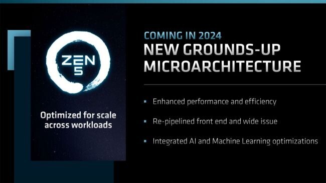
Samsung to Detail SF4X Process for High-Performance Chips

Samsung has invested heavily in semiconductor manufacturing technology to provide clients with a viable alternative to TSMC and its portfolio of nodes spanning anything from mobile to high-performance computing (HPC) applications. Today, we have information that Samsung will present its SF4X node to the public in this year's VLSI Symposium. Previously known as a 4HPC node, it is designed as a 4 nm-class node with a specialized use case for HPC processors, in contrast to the standard SF4 (4LPP) node that uses 4 nm transistors designed for low-power standards applicable to mobile/laptop space. According to the VLSI Symposium schedule, Samsung is set to present more info about the paper titled "Highly Reliable/Manufacturable 4nm FinFET Platform Technology (SF4X) for HPC Application with Dual-CPP/HP-HD Standard Cells."

As the brief introduction notes, "In this paper, the most upgraded 4nm (SF4X) ensuring HPC application was successfully demonstrated. Key features are (1) Significant performance +10% boosting with Power -23% reduction via advanced SD stress engineering, Transistor level DTCO (T-DTCO) and [middle-of-line] MOL scheme, (2) New HPC options: Ultra-Low-Vt device (ULVT), high speed SRAM and high Vdd operation guarantee with a newly developed MOL scheme. SF4X enhancement has been proved by a product to bring CPU Vmin reduction -60mV / IDDQ -10% variation reduction together with improved SRAM process margin. Moreover, to secure high Vdd operation, Contact-Gate breakdown voltage is improved by >1V without Performance degradation. This SF4X technology provides a tremendous performance benefits for various applications in a wide operation range." While we have no information on the reference for these claims, we suspect it is likely the regular SF4 node. More performance figures and an in-depth look will be available on Thursday, June 15, at Technology Session 16 at the symposium.

AMD Ryzen 8000 "Granite Ridge" Zen 5 Processor to Max Out at 16 Cores

AMD's next-generation Ryzen 8000 "Granite Ridge" desktop processor based on the "Zen 5" microarchitecture, will continue to top out at 16-core/32-thread as the maximum CPU core-count possible, says a report by PC Games Hardware. The processor will retain the chiplet design of the current Ryzen 7000 "Raphael" processor, with two 8-core "Zen 5" CCDs, and one I/O die. It's very likely that AMD will reuse the same 6 nm client I/O die (cIOD) as "Raphael," just the way it used the same 12 nm cIOD between Ryzen 3000 "Matisse" and Ryzen 5000 "Vermeer;" but with updates that could enable higher DDR5 memory speeds. Each of the up to two "Eldora" Zen 5 CCDs has 8 CPU cores, with 1 MB of dedicated L2 cache per core, and 32 MB of shared L3 cache. The CCDs are very likely to be built on the TSMC 3 nm EUV silicon fabrication process.

Perhaps the most interesting aspect of the PCGH leak would have to be the TDP numbers being mentioned, which continue to show higher-performance SKUs with 170 W TDP, and lower tiers with 65 W TDP. With its CPU core-counts not seeing increases, AMD would bank on not just the generational IPC increase of its "Zen 5" cores, but also max out performance within the power envelope of the new node, by dialing up clock speeds. AMD could ride out 2023 with its Ryzen 7000 "Zen 4" processors on the desktop platform, with "Granite Ridge" slated to enter production only by Q1-2024. The company could update its product stack in the meantime, perhaps even bring the 4 nm "Phoenix" monolithic APU silicon to the Socket AM5 desktop platform. Ryzen 8000 is expected to retain full compatibility with existing Socket AM5, and AMD 600-series chipset motherboards.

AMD Releases Ryzen 7040U Series "Zen 4" Processors for Ultraportables

AMD today released its Ryzen 7040U series "Zen 4" mobile processors for the Ultraportable segment. These are processors with a 15 W TDP that's configurable up to 30 W by notebook designers to enable better boost frequency residency. AMD technically announced its entire Ryzen 7040 series at the 2023 International CES, but put out details for only the 7040HS series with a 28 W to 45 W TDP targeting thin-and-light and mainstream notebook form-factors. This would be the first time we're seeing details of the 7040U series. The company announced that processors in the 7040U series are shipping to notebook manufacturers, but it did not put out a specific date on which you can buy notebooks powered by these processors.

The Ryzen 7040U series consists of four processor models (SKUs). The lineup is led by the Ryzen 7 7840U, followed by the Ryzen 5 7640U, the Ryzen 5 7540U, and has the Ryzen 3 7440U at the entry level. All four processor models offer the latest "Zen 4" CPU cores and RDNA3 graphics. The Ryzen 7 7840U packs an 8-core/16-thread CPU clocked at 3.30 GHz with up to 5.10 GHz boost frequency. The Ryzen 5 7640U has a 6-core/12-thread CPU clocked at 3.50 GHz with up to 4.90 GHz boost. The Ryzen 5 7540U differs from the 7640U not just in slightly lower CPU clock speeds—3.20 GHz with up to 4.90 GHz boost—but also the lack of the XDNA Ryzen AI feature. The Ryzen 3 7440U has a leaner CPU still, with just 4-core/8-thread, clocked at 3.00 GHz with up to 4.70 GHz boost, half the shared L3 cache size of the other three models, and a lack of Ryzen AI.

Intel Arc Battlemage and Celestial Graphics Architectures Teased by Employees

Intel Graphics employees inadvertently revealed that the company's Xe2 "Battlemage" graphics architecture is being designed for the 4 nm silicon fabrication node, which would give Intel's GPU designers a leap in transistor density and power headroom, given that TSMC 4 nm is an EUV node compared to the current 6 nm DUV node the company builds its Arc "Alchemist" GPUs on. The leak also seems to confirm that its succeeding "Celestial" graphics architecture is being designed for 3 nm. An enthusiast named gamma0burst sifted through public profiles of several Intel employees, and scored these details in their professional profile pages.

We are almost certain that Xe2 "Battlemage" is going to be built on the TSMC 4 nm node, and to a slightly lesser degree, about Xe3 "Celestial" being designed for TSMC's 3 nm N3X node. Intel roadmaps pin the debut of "Battlemage" to a 2023-2024 timeline, although this could also be a reference to the iGPU of the upcoming Core "Meteor Lake" processors that debut in the second half of 2023. Intel is highly likely to deliver "Meteor Lake" within its 2H-2023 timeline, which would mean that the mention of "2024" in the graphics technology roadmap could mean that discrete GPUs based on "Battlemage" only arrive next year.

AMD to Shift Some of its 4 nm CPU Silicon-fabrication to Samsung from TSMC

AMD has reportedly signed up with Samsung Electronics to shift some of its 4 nm processor silicon fabrication from TSMC. The apex Taiwan-based foundry is reportedly operating at capacity for its 4 nm-class nodes, with customers such as Apple and Qualcomm sourcing 4 nm mobile SoCs on the node, leaving AMD with limited allocation and/or bargaining power with TSMC. The company relies on 4 nm for its Ryzen 7040 series "Phoenix" mobile processors, and is in the process of adapting its design for Samsung's 4 nm-class nodes (of which there are five types for AMD to choose from).

Switching to Samsung probably gives AMD more scalability, particularly given that "Phoenix" has missed its release timeline, leaving AMD with the 5 nm + 6 nm Ryzen 7045 series "Dragon Range" MCM in the premium segments, and older 6 nm 7035 series "Rembrandt-R" in the mainstream and ultraportable segments, but nothing "apt" to compete against Intel "Raptor Lake-U" and "Raptor Lake-P." AMD has a limited window in which to ramp up "Phoenix," as Intel readies "Meteor Lake" for a 2H-2023 debut, with a focus on mobile variants.

Report Suggests AMD Ryzen Threadripper 8000 "Shimada Peak" HEDT CPUs Prepped for 2025 Launch

DigiTimes has been informed that many of TSMC's customers are likely to postpone usage of the foundry's 3 nm process node into 2024 or beyond, due to a slowdown in the PC hardware market - insider sources suggest that AMD will be sticking with 4 nm and 6 nm nodes for many of its future CPU lineups. The next generation Zen 5-based family is expected to launch in 2024 - which aligns with information issued by AMD via financial reports - a roadmap (based on DigiTime's findings) points to AMD offering a range of mainstream desktop (Granite Ridge) and laptop/mobile CPUs (Fire Range).

No high-end desktop (HEDT) options are marked for release in 2024, and DigiTimes reckons that AMD is planning to release Zen 5-based Ryzen Threadripper processors in the following year. The codename for the Ryzen Threadripper 8000-series seems to be "Shimada Peak" and industry experts think that these HEDT CPUs will eventually succeed the Threadripper "Storm Peak" 7000 family (due for launch later in 2023) - a shared socket design is also a likelihood due to AMD wanting to stretch out the lifespan of mounting connection standards by avoiding costly decisions - their sTRX4/SP3r3 socket only survived for one generation.

ASUS ROG Ally Powered by AMD Ryzen Z1 Extreme Priced at $700

ASUS's sensational handheld game console, the ROG Ally, will be priced at $699.99 for the model powered by the top AMD Ryzen Z1 Extreme processor, according to a leak by SnoopyTech. This top model will feature a 7-inch Full HD screen with 120 Hz refresh-rate, and Dolby Atmos-capable audio. Under the hood, the Ryzen Z1 is based on the 4 nm "Phoenix" silicon, featuring an 8-core/16-thread "Zen 4" CPU, and its full Navi3 iGPU based on the RDNA3 graphics architecture, with 12 CU (768 stream processors). This chip is wired to 16 GB of LPDDR5 memory, and a 512 GB NVMe SSD.

ASUS has a cheaper model of the ROG Ally designed for cloud gaming and casual gaming, powered by the Ryzen Z1 (non-Extreme). The non-Extreme Z1 rocks a 6-core/12-thread "Zen 4" CPU, but a heavily cut down iGPU with just 4 CU (256 stream processors), which are plenty for the intended use-cases. ASUS could price this much lower than the top model, with speculations pointing to $499.

Qualcomm Snapdragon 8 Gen 3 Differing Core Clusters Revealed in Leak, NUVIA Phoenix-Based Gen 4 Hinted

A technology tipster has been dropping multiple tidbits this week about Qualcomm's upcoming Snapdragon 8 Gen 3 mobile chipset - this follows a leak (from a different source, going back to mid-April) about the next generation Adreno 750 GPU getting tuned up for a battle against Apple's Bionic A17 in terms of graphics benchmarks. The latest leak points to the GPU being clocked at 900 MHz, rather than the rumored higher figure of 1.0 GHz speed (garnered from tests at Qualcomm's labs). The focus has now turned to the next generation flagship Snapdragon's CPU aspect, with information emerging about core clock speeds and multiple cluster configurations.

Revegnus suggests that the Snapdragon 8 Gen 3 (SD8G3) chipset will be packing a large primary core in the shape of Arm's Cortex-X4 CPU with a reported maximum clock speed of 3.40 GHz. Leaks from the past have posited that the SD8G3 would feature a fairly standard 1x Large + 5x Big + 2x Small CPU core layout (with clocks predicted to be: large Cortex X4 at 3.2 GHz, big Cortex-A720 at 3.0 GHz, and small Cortex-A520 at 2.0 GHz). An insider source has provided Revegnus with additional information about two different CPU core configurations - 1+5+2 and 2+4+2 - it is theorized that smartphone manufacturers will be offered the latter layout as an exclusive option for special edition flagship phones. The more powerful 2+4+2 variant is said to sacrifice a big core (A720) in favor of a dual Cortex X4 headliner, although the resultant thermal output of twin large cores could prove to be problematic.

MediaTek's Dimensity 9300 SoC Predicted to Have Fighting Chance Against Snapdragon 8 Gen 3

Early details of MediaTek's next generation mobile chipset have emerged this week, courtesy of renowned leaker Digital Chat Station via their blog on Weibo. The successor to MediaTek's current flagship Dimensity 9200 mobile chipset will likely be called "Dimensity 9300" - a very imaginative bump up in numbering - with smartphone brand Vivo involved as a collaborator. The tipster thinks that the fabless semiconductor company has contracted with TSMC for fabrication of the Dimensity 9300 chipset - and the foundry's N4P process has been selected by MediaTek, which could provide a bump in generational performance when compared to the older 4 nm and 5 nm standards used for past Dimensity SoC ranges. It should be noted that the current generation Dimensity 9200 chipset is presently manufactured via TSMC's N4P process.

MediaTek is seeking to turnaround its fortunes in the area of flagship mobile chipsets - industry watchdogs have cited a limited uptake of the Taiwanese company's Dimensity 9200 SoC as a motivating factor in the creation of a very powerful successor. Digital Chat Station suggests that the upcoming 9300 model will pack enough of a hardware punch to rival Qualcomm's forthcoming Snapdragon 8 Gen 3 SoC - both chipsets are touted to release within the same time period of late 2023. According to previous speculation, Qualcomm has also contracted with TSMC's factory to pump out the Snapdragon 8 Gen 3 via the N4P (4 nm) process.

Strict Restrictions Imposed by US CHIPS Act Will Lower Willingness of Multinational Suppliers to Invest

TrendForce reports that the US Department of Commerce recently released details regarding its CHIPS and Science Act, which stipulates that beneficiaries of the act will be restricted in their investment activities—for more advanced and mature processes—in China, North Korea, Iran, and Russia for the next ten years. The scope of restrictions in this updated legislation will be far more extensive than the previous export ban, further reducing the willingness of multinational semiconductor companies to invest in China for the next decade.

CHIPS Act will mainly impact TSMC; and as the decoupling of the supply chain continues, VIS and PSMC capture orders rerouted from Chinese foundries
In recent years, the US has banned semiconductor exports and passed the CHIPS Act, all to ensure supply chains decoupling from China. Initially, bans on exports were primarily focused on non-planar transistor architecture (16/14 nm and more advanced processes). However, Japan and the Netherlands have also announced that they intend to join the sanctions, which means key DUV immersion systems, used for producing both sub-16 nm and 40/28 nm mature processes, are likely to be included within the scope of the ban as well. These developments, in conjunction with the CHIPS Act, mean that the expansion of both Chinese foundries and multinational foundries in China will be suppressed to varying degrees—regardless of whether they are advanced or mature processes.

Snapdragon 8 Gen 3 GPU Could be 50% More Powerful Than Current Gen Adreno 740

An online tipster, posting on the Chinese blog site Weibo, has let slip that Qualcomm's upcoming Snapdragon 8 Gen 3 mobile chipset is touted to pack some hefty graphical capabilities. The suggested Adreno "750" smartphone and tablet GPU is touted to offer a 50% increase over the present generation Adreno 740 - as featured on the recently released and cutting-edge Snapdragon 8 Gen 2 chipset. The current generation top-of-the-range Snapdragon is no slouch when it comes to graphics benchmarks, where it outperforms Apple's prime contender - the Bionic A16 SoC.

The Snapdragon 8 Gen 3 SoC is expected to launch in the last quarter of 2023, but details of the flagship devices that it will power are non-existent at the time of writing. The tipster suggests that Qualcomm has decided to remain on TSMC's 4 nm process for its next generation mobile chipset - perhaps an all too safe decision when you consider that Apple has upped the stakes with the approach of its Bionic A17 SoC. It has been reported that the Cupertino, California-based company has chosen to fabricate via TSMC's 3 nm process, although the Taiwanese foundry is said to be struggling with its N3 production line. The engineers at Qualcomm's San Diego headquarters are alleged to be experimenting with increased clock speeds running on the next gen Adreno GPU - as high as 1.0 GHz - in order to eke out as much performance as possible, in anticipation of besting the Bionic A17 in graphics benchmarks. The tipster theorizes that Qualcomm will still have a hard time matching Apple in terms of pure CPU throughput, so the consolation prize will lie with a superior GPU getting rigged onto the Snapdragon 8 Gen 3.

Intel's Next Generation GPUs to be Made by TSMC, Celestial Set for 3 nm Process

Intel has awarded TSMC with some big contracts for future manufacturing of next generation GPUs, according to Taiwan's Commercial Times. As previously covered on TPU, the second generation Battlemage graphics processing units will get fabricated via a 4 nm process. According to insider sources at both partnering companies, Intel is eyeing a release date in the second half of 2024 for this Xe2-based architecture. The same sources pointed to the third generation Celestial graphics processing units being ready in time for a second half of 2026 launch window. Arc Celestial, which is based on the Xe3 architecture, is set for manufacture in the coming years courtesy of TSMC's N3X (3 nm) process node.

One of the sources claim that Intel is quietly confident about its future prospects in the GPU sector, despite mixed critical and commercial reactions to the first generation line-up of Arc Alchemist discrete graphics cards. The company is said to be anticipating great demand for more potent versions of its graphics products in the future, and internal restructuring efforts have not dulled the will of a core team of engineers. The restructuring process resulted in the original AXG graphics division being divided into two sub-groups - CCG and DCAI. The pioneer of the entire endeavor, Raja Koduri, departed Intel midway through last month, to pursue new opportunities with an AI-focused startup.

Intel Arc "Battlemage" to Double Shader Count, Pack Larger Caches, Use TSMC 4 nm

Intel's next-generation Arc "Battlemage" GPU is expected to numerically-double its shader counts, according to a report by RedGamingTech. The largest GPU from the Arc "Battlemage" series, the "BMG-G10," aims to power SKUs that compete in the performance segment. The chip is expected to be built on a TSMC 4 nm-class EUV node, similar to NVIDIA's GeForce "Ada" GPUs, and have a die-size similar to that of the "AD103" silicon powering the GeForce RTX 4080.

Among the juiciest bits from this report are that the top "Battlemage" chip will see its Xe Core count doubled to 64, up from 32 on the top "Alchemist" part. This would see its execution unit (EU) count doubled to 1,024, and unified shader counts at 8,192. Intel is expected to give the chip clock speeds in excess of 3.00 GHz. The Xe Cores themselves could see several updates, including IPC uplifts, and support for new math formats. The memory sub-system is expected to see an overhaul, with a large 48 MB on-die L2 cache. While the memory bus is unchanged at 256-bit wide, the memory speed could see a significant increase up from the 16-17.5 Gbps on the Arc A770. As for when customers can actually expect products, the RedGamingTech report puts launch of the Arc "Battlemage" series at no sooner than Q2-2024. The company is expected to launch refreshed "Alchemist+" GPUs in 2023.

AMD Ryzen 7 7840U Low-Power Processor Beats Previous-Gen Flagship Ryzen 9 6900HX

AMD's 4 nm "Phoenix" silicon could serious turn the company's fortunes around in the ultra-thin notebook space. The 28-Watt Ryzen 7 7840U surfaced on Cinebench R23 screenshots, where it is shown beating the previous-generation 55 W flagship, the Ryzen 9 6900HX. If this is any indication of performance across the board, then the 15-28 W models of Ryzen 7040-series "Phoenix" could unleash an open-season against competing 15-28 W-category 13th Gen Core processors that have lower P-core counts, such as 2P+8E. The 7840U has all eight "Zen 4" CPU cores enabled, along with a fast RDNA3 graphics architecture based iGPU. In the screenshot, the 7840U is shown with a Cinebench R23 multi-threaded score of 14285 points, a score that is higher than that of the "Zen 3+" based 6900HX "Rembrandt," and a touch below the 45 W Core i7-12800H, which means it could have the upper hand over several 13th Gen and 12 Gen SKUs in the 15-28 W category.

Samsung Preps Mass Production of Third-Generation 4 nm Chipsets, Start Date Expected Mid-2023

In a Samsung Electronics business report released on March 12, it was revealed that the giant electronics manufacturer will begin mass production of new chips through a 4 nm 2.3-generation process. The newly established manufacturing process is set to start by the end of H1 2023, which means that mid-June would be the expected commencement date. Samsung Semiconductor has managed to produce a satisfactory yield of wafers with the new generation chipsets.

Samsung Electronics has experienced significant problems with the production of previous generation 4 nm chips, and industry insiders have been surprised by the sudden announcement of the third generation version, given rumors pointing to the Hwaseong factory struggling to reach yields at the 60% mark. Qualcomm famously dropped Samsung in favor of TSMC as a source of 4 nm chipsets in 2022, due to disappointing yield figures.

TSMC's 3 nm Node at Near 50 Percent Utilisation, Other Nodes Seeing Lower Demand

Based on multiple reports out of Taiwan, TSMC is seeing increased utilisation of its 3 nm node and its production line is now at close to 50 percent utilisation. The main customer here is without a doubt Apple and TSMC is churning out some 50-55,000 wafers a month on its 3 nm node. TSMC is also getting ready to start production on its N3E node later this year, which will see some customers move to the node.

However, it's not all good news, as TSMC is seeing a decline in utilisation on its 5/4 and 7/6 nm nodes as demand has dropped significantly here, with different news outlets reporting different figures. Some are suggesting the 7/6 nm nodes might have dropped as low as to 50 percent utilisation, others mention 70 percent. The 5/4 nm nodes aren't anywhere nearly as badly affected and remain at around 80 percent utilisation. The good news for TSMC is that this is expected to be a temporary slump in demand and most of its leading edge nodes should be back at somewhere around a 90 percent utilisation rate by the second half of the year. However, this depends on what the demand for its partners' products will look like going forward, as many of TSMC's customers are seeing lower demand for their products in turn.

Samsung Electronics Announces Fourth Quarter and FY 2022 Results, Profits at an 8-year Low

Samsung Electronics today reported financial results for the fourth quarter and the fiscal year 2022. The Company posted KRW 70.46 trillion in consolidated revenue and KRW 4.31 trillion in operating profit in the quarter ended December 31, 2022. For the full year, it reported 302.23 trillion in annual revenue, a record high and KRW 43.38 trillion in operating profit.

The business environment deteriorated significantly in the fourth quarter due to weak demand amid a global economic slowdown. Earnings at the Memory Business decreased sharply as prices fell and customers continued to adjust inventory. The System LSI Business also saw a decline in earnings as sales of key products were weighed down by inventory adjustments in the industry. The Foundry Business posted a new record for quarterly revenue while profit increased year-on-year on the back of advanced node capacity expansion as well as customer base and application area diversification.

Intel Foundry Services Onboards a Fabless Customer, Deal Expected to Fetch over $4 Billion

Intel Foundry Services, the semiconductor foundry business of Intel, has onboarded an undisclosed fabless customer, the company disclosed in its Q4-2022 Financial Results presentation. This signals that the company wants to serve the semiconductor manufacturing industry beyond its own products, and scale up to demands, just like TSMC, UMC, Samsung Foundry, or other such semiconductor foundries do. The customer is looking to build chips on the Intel 3 foundry-node, which is rumored to offer performance/Watt and transistor-density figures comparable to TSMC 4N (4 nm EUV). Intel will extensively use Tower Semiconductor's silicon fabrication IP in the deal. Throughout its manufacturing lifecycle (from risk production to mass-production and completion), the deal is expected by Intel to generate over $4 billion in revenue for the company.
Image Courtesy: VideoCardz

Intel Xeon "Sapphire Rapids" to be Quickly Joined by "Emerald Rapids," "Granite Rapids," and "Sierra Forest" in the Next Two Years

Intel's server processor lineup led by the 4th Gen Xeon Scalable "Sapphire Rapids" processors face stiff competition from AMD 4th Gen EPYC "Genoa" processors that offer significantly higher multi-threaded performance per Watt on account of a higher CPU core-count. The gap is only set to widen, as AMD prepares to launch the "Bergamo" processor for cloud data-centers, with core-counts of up to 128-core/256-thread per socket. A technologically-embattled Intel is preparing quick counters as many as three new server microarchitecture launches over the next 23 months, according to Intel, in its Q4-2022 Financial Results presentation.

The 4th Gen Xeon Scalable "Sapphire Rapids," with a core-count of up to 60-core/120-thread, and various application-specific accelerators, witnessed a quiet launch earlier this month, and is shipping to Intel customers. The company says that it will be joined by the Xeon Scalable "Emerald Rapids" architecture in the second half of 2023; followed by "Granite Rapids" and "Sierra Forest" in 2024. Built on the same LGA4677 package as "Sapphire Rapids," the new "Emerald Rapids" MCM packs up to 64 "Raptor Cove" CPU cores, which support higher clock-speeds, higher memory speeds, and introduce the new Intel Trust Domain Extensions (TDX) instruction-set. The processor retains the 8-channel DDR5 memory interface, but with higher native memory speeds. The chip's main serial interface is a PCI-Express Gen 5 root-complex with 80 lanes. The processor will be built on the last foundry-level refinement of the Intel 7 node (10 nm Enhanced SuperFin); many of these refinements were introduced with the company's 13th Gen Core "Raptor Lake" client processors.

NVIDIA GeForce RTX 4060 Ti Possible Specs Surface—160 W Power, Debuts AD106 Silicon

NVIDIA's next GeForce RTX 40-series "Ada" graphics card launch is widely expected to be the GeForce RTX 4070 (non-Ti), and as we approach Spring 2023, the company is expected to ramp up to the meat of its new generation, with xx60-segment, beginning with the GeForce RTX 4060 Ti. This new performance-segment SKU debuts the 4 nm "AD106" silicon. A set of leaks by kopite7kimi, a reliable source with NVIDIA leaks, shed light on possible specifications.

The RTX 4060 Ti is based on the AD106 silicon, which is expected to be much smaller than the AD104 powering the RTX 4070 series. The reference board developed at NVIDIA, codenamed PG190, is reportedly tiny, and yet it features the 16-pin ATX 12VHPWR connector. This is probably set for 300 W at its signal pins, and adapters included with graphics cards could convert two 8-pin PCIe into one 300 W 16-pin connector. The RTX 4060 Ti is expected to come with a typical graphics power value of 160 W.

GALAX GeForce RTX 4070 (non-Ti) Graphics Cards Pictured

Marketing pictures of two custom-design GeForce RTX 4070 "Ada" (non-Ti) graphics card models by GALAX, were leaked to the web. The more simple-looking of the two is very likely the GALAX RTX 4070 EX Gamer White; while the other more flashy of the two, could be the GALAX RTX 4070 SG White. What's interesting is that both cards are triple-slot, including with their I/O brackets, for what is supposed to be a mid performance-segment product positioned below the recently launched RTX 4070 Ti.

Rumored specifications of the RTX 4070 (non-Ti) have it, that the SKU is based on the same 4 nm "AD104" silicon as the RTX 4070 Ti, albeit significantly cut-down, with only 46 out of 60 streaming multiprocessors (SM) on the silicon being enabled (that's 76% of the available SIMD machinery). This works out to 5,888 CUDA cores, 46 RT cores, and 184 Tensor cores. The card might get the same 12 GB memory size, across the 192-bit GDDR6X memory bus of the AD104, with the same 21 Gbps memory speed, working out to 504 GB/s bandwidth. One reason why GALAX's cards look this buff could have to do with NVIDIA's partners reusing their RTX 4070 Ti board designs for their premium RTX 4070 cards.

AMD Ryzen 7040 Series "Phoenix Point" Mobile Processor I/O Detailed: Lacks PCIe Gen 5

The online datasheets of some of the first AMD Ryzen 7040 series "Phoenix Point" mobile processors went live, detailing the processor's I/O feature-set. We learn that AMD has decided to give PCI-Express Gen 5 a skip with this silicon, at least in its mobile avatar. The Ryzen 7040 SoC puts out a total of 20 PCI-Express Gen 4 lanes, all of which are "usable" (i.e. don't count 4 lanes toward chipset-bus). This would mean that the silicon has a full PCI-Express 4.0 x16 interface for discrete graphics, and a PCI-Express 4.0 x4 link for a CPU-attached M.2 NVMe slot; unlike the "Raphael" desktop MCM and the "Dragon Range" mobile MCM, whose client I/O dies put out a total of 28 Gen 5 lanes (24 usable, with x16 PEG + two x4 toward CPU-attached M.2 slots).

Another interesting aspect about "Phoenix Point" is its memory controllers. The SoC features a dual-channel (four sub-channel) DDR5 memory interface, besides support for LPDDR5 and LPDDR5x. DDR5-5600 and LPDDR5-7600 are the native speeds supported. What's really interesting is the maximum amount of memory supported, which stands at 256 GB—double that of "Raphael" and "Dragon Range," which top out at 128 GB. This bodes well for the eventual Socket AM5 APUs AMD will design based on the "Phoenix Point" silicon. Older Ryzen 5000G "Cezanne" desktop APUs are known for superior memory overclocking capabilities to 5000X "Vermeer," with the monolithic nature of the silicon favoring latencies. Something similar could be expected from "Phoenix Point."

AMD Announces Ryzen 7040 "Phoenix Point" Mobile Processor: 4nm, Zen 4, RDNA3, XDNA

AMD today launched two distinct kinds of mobile processors, the Ryzen 7045 "Dragon Range" serves the 45 W H- and HX-segments of performance and enthusiast notebooks with CPU core counts of up to 16-core/32-thread; while the U-segment, P-segment, and a portion of the H-segment (ranges of 15 W, 28 W, and 35 W), will be led by the Ryzen 7040 "Phoenix Point." Unlike the "Dragon Range" MCM, "Phoenix Point" is a monolithic silicon built entirely on the TSMC 4 nm EUV foundry node, and introduces a wealth of process-level and system-level power-management features.

AMD "Phoenix Point" combines an 8-core/16-thread CPU based on the "Zen 4" microarchitecture, with a powerful iGPU based on the latest RDNA3 graphics architecture, and a feature-packed AI acceleration engine based on the XDNA architecture AMD built after the Xilinx acquisition. The CPU component is a fully-fledged "Zen 4" CCX, with 8 CPU cores featuring 1 MB of dedicated L2 cache per-core, and sharing a large 32 MB L3 cache. This is an increase from the previous generation "Rembrandt" and "Cezanne" dies that had a reduced 16 MB L3 shared among the eight "Zen 3" or "Zen 3+" CPU cores.

NVIDIA GeForce RTX 4070 Ti to Launch $100 Cheaper Than RTX 4080 12 GB

A leaked NVIDIA company slide confirms that the upcoming GeForce RTX 4070 Ti graphics card will launch at a starting price of USD $799. This would put it $100 cheaper than what was going to be the launch price of the RTX 4080 12 GB. NVIDIA cancelled the launch of the RTX 4080 12 GB, and reportedly re-branded it to the RTX 4070 Ti. The RTX 4080 12 GB was supposed to launch alongside the RTX 4080 16 GB in mid-November 2022, but the company decided to "unlaunch" it, in the wake of bad press on the confusing and deceptive naming of the SKU, and its ambitious MSRP that would have put custom-design cards well above the $1,000-mark.

The NVIDIA slide goes on to claim that the RTX 4070 Ti will be faster than the previous-generation flagship, the RTX 3090 Ti. This is thanks to its 40 shader TFLOP/s, 93 RT TFLOP/s, and 642 Tensor TFLOP/s. The RTX 4070 Ti is expected to debut the new 4 nm "AD104" silicon, featuring 7,680 CUDA cores, 60 RT cores, 240 Tensor cores, 240 TMUs, and 80 ROPs. The card features 12 GB of 21 Gbps GDDR6X memory across a rather narrow 192-bit memory bus. The slide confirms that January 5, 2023 will be the market availability date for the RTX 4070 Ti. NVIDIA's decision to price the RTX 4070 Ti at $799 may have been influenced by the AMD Radeon RX 7900 XT priced at $899.

Top 10 TSMC Customers Said to have Cut Orders for 2023

On the day of TSMC's celebration of the mass production start of its 3 nm node, news out of Taiwan suggests that all of its top 10 customers have cut their orders for 2023. However, the cuts are unlikely to affect its new node, but rather its existing nodes, with the 7 and 6 nm nodes said to be hit the hardest, by as much as a 50 percent utilisation reduction in the first quarter of 2023. The 28 nm and 5 and 4 nm nodes are also said to be affected, although it's unclear by how much at this point in time.

Revenue is expected to fall by at least 15 percent in the first quarter of 2023 for TSMC, based on numbers from DigiTimes. The fact that TSMC has increased its 2023 pricing by six percent should at least help offset some of the potential losses for the company, but it all depends on the demand for the rest of the year. Demand for mobile devices is down globally, which is part of the reason why so many of TSMC's customers have cut back their orders, as Apple, Qualcomm and Mediatek all produce their mobile SoCs at TSMC. Add to this that the demand for computers and new computer components are also down, largely due to the current pricing and TSMC is in for a tough time next year.
Return to Keyword Browsing
May 21st, 2024 16:08 EDT change timezone

New Forum Posts

Popular Reviews

Controversial News Posts