MINISFORUM Formally Launches V3 High-Performance AMD AI 3-in-1 Tablet
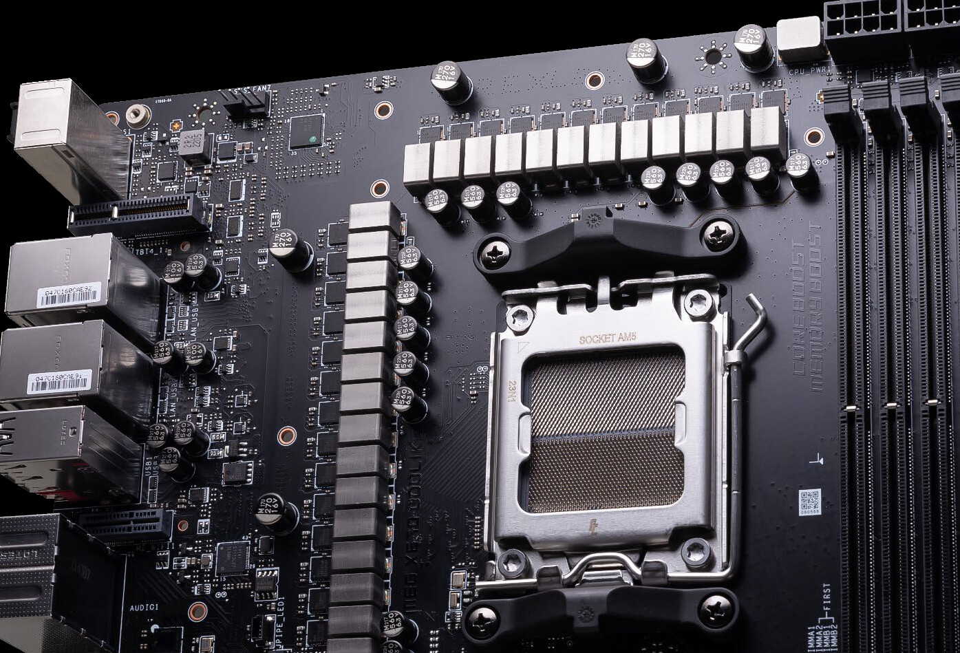
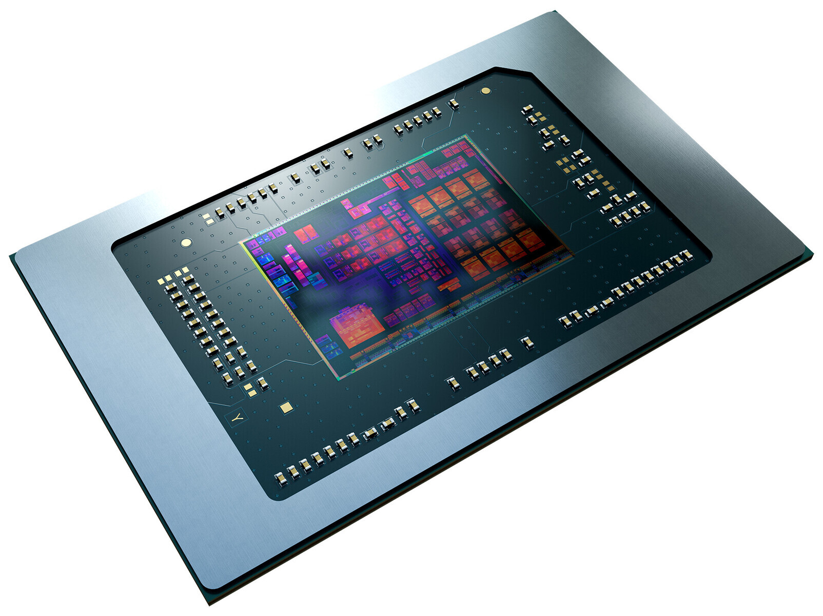
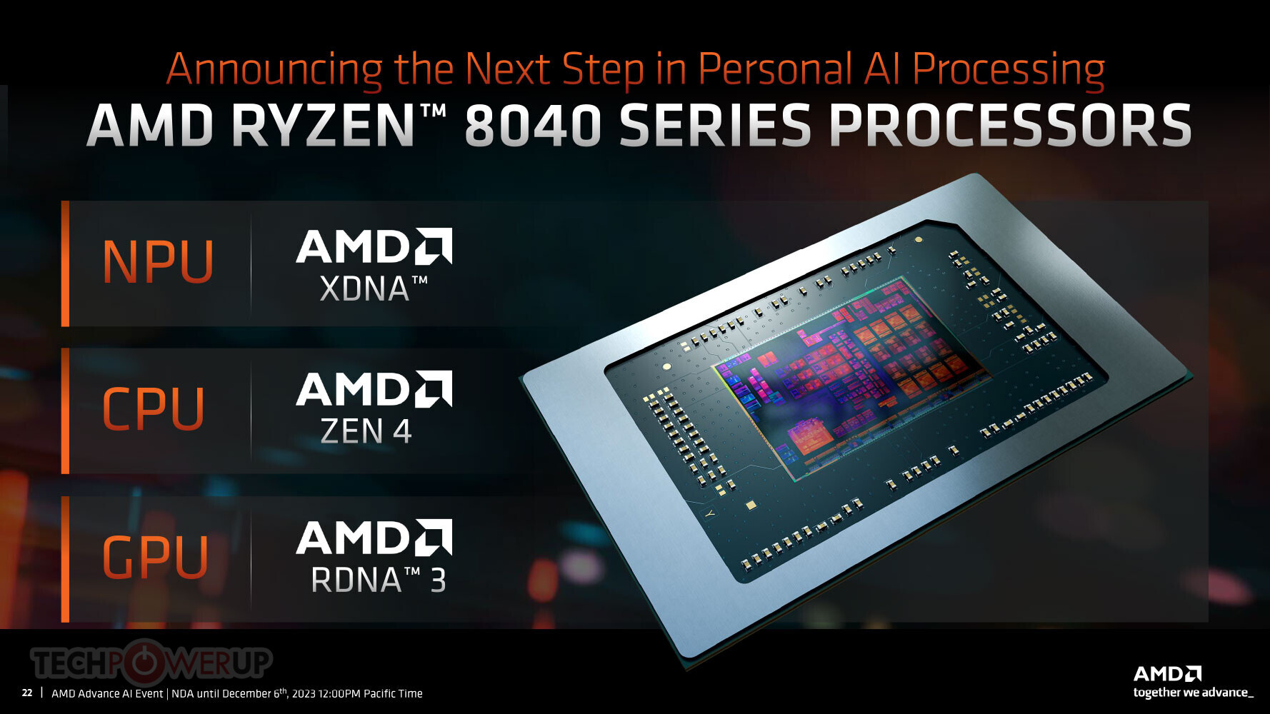
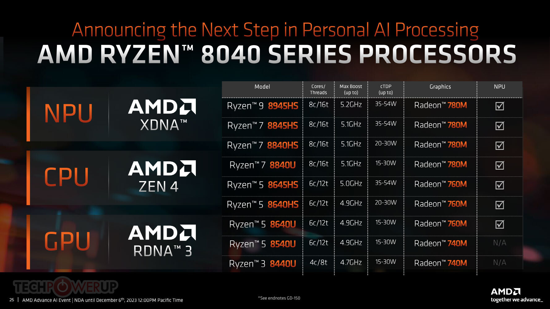
Recently, MINISFORUM updated the CPU of V3 to AMD's latest Ryzen7 8840U on its official website. Previously, the preview page for V3 went live on January 3rd. It is understood that MINISFORUM is expected to hold the V3 and Spring New Product Launch Event at the end of March 2024. MINISFORUM V3 is the world's first high-performance AMD AI 3-in-1 tablet, featuring AMD's latest Ryzen7 8840U, built on a 4 nm process, with Zen 4 CPU and RDNA3 GPU architecture, 8 cores 16 threads, a base frequency of 3.30 GHz, and a maximum boost frequency of 5.10 GHz, with a TDP of 15-30 W, and a 16 MB L3 cache. It integrates Radeon 780M graphics. V3 also boasts a dual-fan and four-copper-pipe cooling system, achieving 28 W sustained performance release, providing sustained power for AI model training, graphic rendering, video editing, and gaming entertainment.
The AMD 8840U is also paired with a proprietary XDNA AI processor, with NPU computing power up to 16TOPS and processor computing power up to 38TOPS. Based on this, V3 is equipped with a new AMD Ryzen AI, creating an AI Windows triple-in-one tablet PC with the highest security level from Microsoft, supporting Microsoft Real-time Communication, and hardware design supporting Microsoft Copilot, which can be called upon with a single click, providing real-time intelligent suggestions and assistance, helping users easily complete tasks in various scenarios for efficient office work.


The AMD 8840U is also paired with a proprietary XDNA AI processor, with NPU computing power up to 16TOPS and processor computing power up to 38TOPS. Based on this, V3 is equipped with a new AMD Ryzen AI, creating an AI Windows triple-in-one tablet PC with the highest security level from Microsoft, supporting Microsoft Real-time Communication, and hardware design supporting Microsoft Copilot, which can be called upon with a single click, providing real-time intelligent suggestions and assistance, helping users easily complete tasks in various scenarios for efficient office work.