News Posts matching #Fab

Return to Keyword Browsing

Magnitude 7.4 Earthquake in Taiwan Halts Production at TSMC and Other Foundries

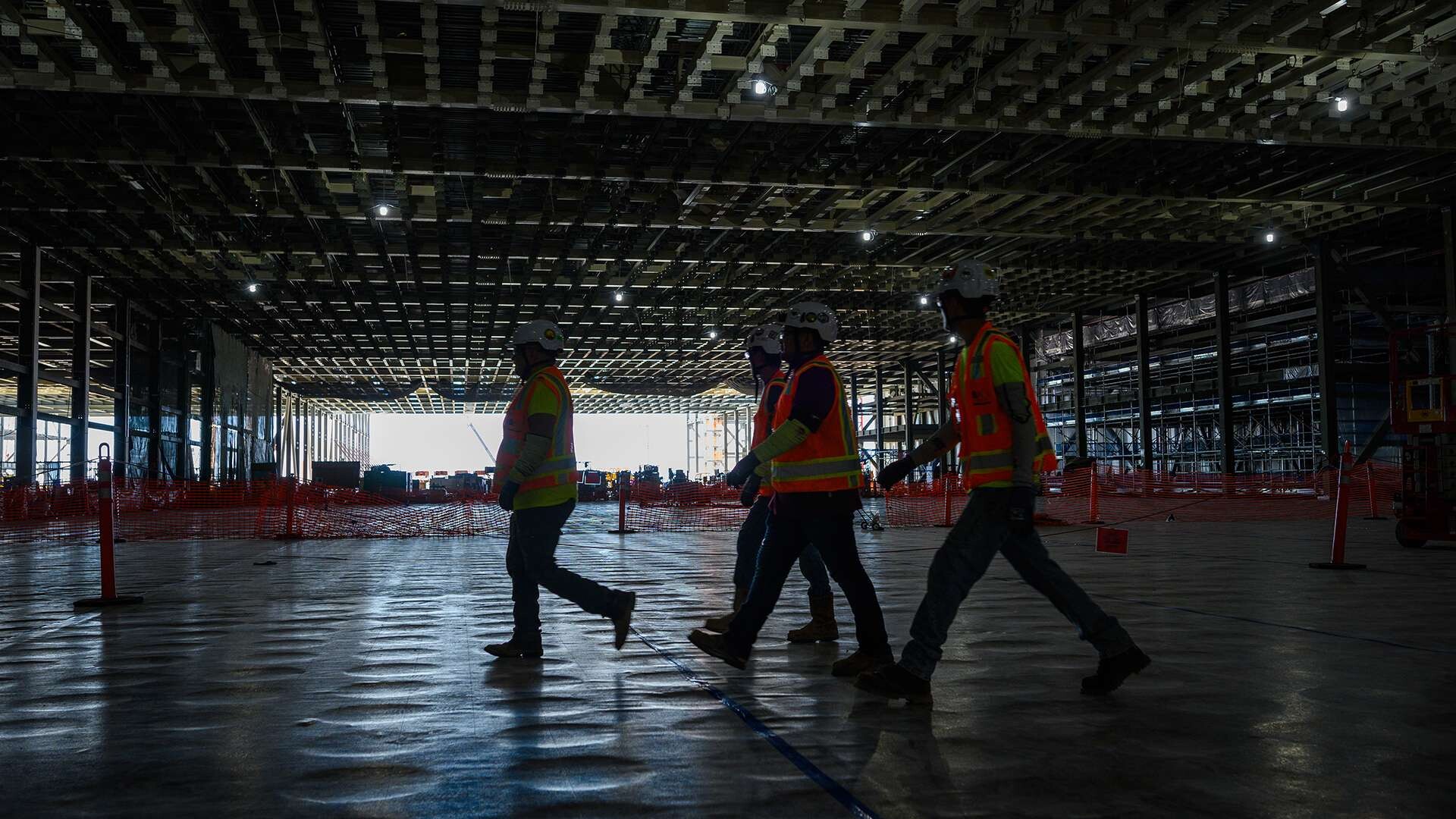
At 07:58 local time, Taiwan was rocked by a magnitude 7.4 earthquake on the east coast which was felt nationwide and as far as to the southeastern parts of China and southern Japan. It caused some major damage in the east coast city of Hualien where the epicentre of the quake was located, as well as surrounding areas. The earthquake reportedly left nine people dead and over 900 people injured islandwide. TSMC, UMC, PSMC and Innolux all halted some of their production lines in the Hsinchu Science Park on the west coast of the island, although this is said to have been as a preventive step, rather than caused by actual damage from the earthquake.

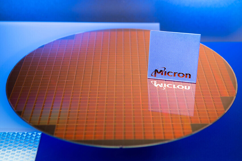
All the above-mentioned companies also evacuated their staff from their factories due to the intensity of the quake, as it reached a magnitude of around four or five almost island wide. The semiconductor manufacturers are all inspecting their fabs now to make sure none of the equipment was damaged by the earthquake. Innolux also has a factory in the southern city of Kaohsiung and has reported that it has suspended production in Hsinchu, but that production in Kaohsiung wasn't affected. Local media in Taiwan hasn't made any mention of the likes of Micron or other chip manufacturers, but it's likely that the situation is similar, since all of these companies are located in the same areas on the island. Aftershocks have continued throughout the day and there's a risk for further big earthquakes to follow in the coming days.
Images courtesy of the Taiwan Central Weather Administration (CWA).

Update 15:11 UTC: Updated with an official statement from Micron below.

Report: Intel Seeks $2 Billion in Funding for Ireland Fab 34 Expansion

According to a Bloomberg report, Intel is seeking to raise at least $2 billion in equity funding from investors for expanding its fabrication facility in Leixlip, Ireland, known as Fab 34. The chipmaker has hired an advisor to find potential investors interested in providing capital for the project. Fab 34 is currently Intel's only chip plant in Europe that uses cutting-edge extreme ultraviolet (EUV) lithography. It produces processors on the Intel 4 process node, including compute tiles for Meteor Lake client CPUs and expected future Xeon data center chips. While $2 billion alone cannot finance the construction of an entirely new fab today, it can support meaningful expansion or upgrades of existing capacity. Intel likely aims to grow Fab 34's output and/or transition it to more advanced 3 nm-class technologies like Intel 3, Intel 20A, or Intel 18A.

Expanding production aligns with Intel's needs for its own products and its Intel Foundry Services business, providing contract manufacturing. Intel previously secured a $15 billion investment from Brookfield Infrastructure for its Arizona fabs in exchange for a 49% stake, demonstrating the company's willingness to partner to raise capital for manufacturing projects. The Brookfield deal also set a precedent of using outside financing to supplement Intel's own spending budget. It provided $15 billion in effectively free cash flow Intel can redirect to other priorities like new fabs without increasing debt. Intel's latest fundraising efforts for the Ireland site follow a similar equity investment model that leverages outside capital to support its manufacturing expansion plans. Acquiring High-NA EUV machinery for manufacturing is costly, as these machines can reach up to $380 million alone.

Report: Global Semiconductor Capacity Projected to Reach Record High 30 Million Wafers Per Month in 2024

Global semiconductor capacity is expected to increase 6.4% in 2024 to top the 30 million *wafers per month (wpm) mark for the first time after rising 5.5% to 29.6 wpm in 2023, SEMI announced today in its latest quarterly World Fab Forecast report.

The 2024 growth will be driven by capacity increases in leading-edge logic and foundry, applications including generative AI and high-performance computing (HPC), and the recovery in end-demand for chips. The capacity expansion slowed in 2023 due to softening semiconductor market demand and the resulting inventory correction.

Ansys Collaborates with TSMC and Microsoft to Accelerate Mechanical Stress Simulation for 3D-IC Reliability in the Cloud

Ansys has collaborated with TSMC and Microsoft to validate a joint solution for analyzing mechanical stresses in multi-die 3D-IC systems manufactured with TSMC's 3DFabric advanced packaging technologies. This collaborative solution gives customers added confidence to address novel multiphysics requirements that improve the functional reliability of advanced designs using TSMC's 3DFabric, a comprehensive family of 3D silicon stacking and advanced packaging technologies.

Ansys Mechanical is the industry-leading finite element analysis software used to simulate mechanical stresses caused by thermal gradients in 3D-ICs. The solution flow has been proven to run efficiently on Microsoft Azure, helping to ensure fast turn-around times with today's very large and complex 2.5D/3D-IC systems.

Texas Instruments Breaks Ground on New 300-mm Semiconductor Wafer Fabrication Plant in Utah

Texas Instruments (TI) today broke ground on its new 300-mm semiconductor wafer fabrication plant (or "fab") in Lehi, Utah. Joined by Utah Governor Spencer Cox, state and local elected officials, as well as community leaders, TI President and Chief Executive Officer Haviv Ilan celebrated the first steps toward construction of the new fab, LFAB2, which will connect to the company's existing 300-mm wafer fab in Lehi. Once completed, TI's two Utah fabs will manufacture tens of millions of analog and embedded processing chips every day at full production.

"Today we take an important step in our company's journey to expand our manufacturing footprint in Utah. This new fab is part of our long-term, 300-mm manufacturing roadmap to build the capacity our customers will need for decades to come," said Ilan. "At TI, our passion is to create a better world by making electronics more affordable through semiconductors. We are proud to be a growing member of the Utah community, and to manufacture analog and embedded processing semiconductors that are vital for nearly every type of electronic system today."

Vietnam is Aiming to Become a Semiconductor Manufacturing Nation

According to a news post by Reuters, Vietnam is the latest nation that is trying to become a semiconductor manufacturing nation, albeit its plans are nothing like what China is doing, instead the nation is trying to woo existing semiconductor companies to build fabs in Vietnam. The nation has been building its high-tech industry over a few years now and although it's nowhere near some of its neighbouring nations, Vietnam is likely to become an important player when it comes to assembly in the not too distant future, alongside India. However, fabricating semiconductors is a big leap from assembling smartphones, computers and EVs and requires a highly skilled workforce, something which is already becoming an issue in nations like Taiwan and Singapore.

Reuters reports that Vietnam has approached both GlobalFoundries and Taiwanese Powerchip Semiconductor Manufacturing Corporation, or PSMC for short. PSMC is among the top 10 foundries in the world, despite only having a mere five fabs, all of which are located in Taiwan. PSMC's main focus is the automotive industry and might be the more likely candidate to consider Vietnam of the two. Neither company has made any kind of commitment to invest in Vietnam. However, building a fab in a nation that doesn't have a semiconductor industry brings with it several challenges, least not supply chain related ones. Reuters mentioned a speech by Synopsys VP Robert Li which he held at the Vietnam Semiconductor Summit, where he mentions that building a foundry in Vietnam might cost as much as US$50 billion, which doesn't seem like a very appealing proposal to any company considering opening up a foundry in the nation.

China's Share in Mature Process Capacity Predicted to Hit 29% in 2023, Climbing to 33% by 2027

TrendForce reports that from 2023 to 2027, the global ratio of mature (>28 nm) to advanced (<16 nm) processes is projected to hover around 7:3. Propelled by policies and incentives promoting local production and domestic IC development, China's mature process capacity is anticipated to grow from 29% this year to 33% by 2027. Leading the charge are giants like SMIC, HuaHong Group, and Nexchip, while Taiwan's share is estimated to consolidate from 49% down to 42%.

Expansion predominantly targets specialty processes such as Driver ICs, CIS/ISPs, and Power Discretes, with second and third-tier Taiwanese manufacturers at the forefront
Within the Driver IC sector, the spotlight is on high voltage (HV) specialty processes. As companies aggressively pursue the 40/28 nm HV process, UMC currently dominates, trailed by GlobalFoundries. Yet, SMIC's 28HV and Nexchip's 40HV are gearing up for mass production in 4Q23 and 1H24, respectively—narrowing their technological gap with other foundries. Notably, competitors with similar process capabilities and capacities, such as PSMC, and those without twelve-inch factories like Vanguard and DBHitek, are poised to face challenges head-on in the short term. This trend may also have long-term implications for UMC and GlobalFoundries.

Intel's Arizona Expansion Marks Construction Milestone

Marking a milestone in Intel's ongoing manufacturing expansion in Arizona, the company today announced that the initial portion of the cleanroom is "weather tight" and the "blow down" phase has begun at the company's two new leading-edge chip factories on its Ocotillo campus in Chandler, Arizona. This milestone underscores Intel's dedication to advancing its presence in the state and fostering technological innovation.

"Our commitment to Arizona runs deep, and as we expand our operations, we remain dedicated to addressing the growing demand for semiconductors and helping the United States regain its leadership position in this vital industry. This milestone represents the result of great teamwork, proficient teams and exceptional craftsmanship of the tradespeople, and it's thanks to their hard work that we've made such significant progress on our site while keeping our culture of caring and the safety of all as our top priority." -Dan Doron, Intel vice president and general manager of Fab Construction Enterprise

Zero ASIC Democratizing Chip Making

Zero ASIC, a semiconductor startup, came out of stealth today to announce early access to its one-of-a-kind ChipMaker platform, demonstrating a number of world firsts:
  • 3D chiplet composability enabling billions of new silicon products
  • Fully automated no-code chiplet-based chip design
  • Zero install interactive RTL-based chip emulation
  • Roadmap to 100X reduction in chip development costs
"Custom Application Specific Integrated Circuits (ASICs) offer 10-100X cost and energy advantage over commercial off the shelf (COTS) devices, but the enormous development cost makes ASICs non-viable for most applications," said Andreas Olofsson, CEO and founder of Zero ASIC. "To build the next wave of world changing silicon devices, we need to reduce the barrier to ASICs by orders of magnitude. Our mission at Zero ASIC is to make ordering an ASIC as easy as ordering catalog parts from an electronics distributor."

Micron Initiates Construction on Leading-Edge Memory Manufacturing Fab

Micron Technology, Inc., one of the world's largest semiconductor companies and the only U.S.-based manufacturer of memory, will today celebrate the start of construction on the nation's first new memory manufacturing fab in 20 years. Company executives will join Idaho Governor Brad Little, Boise Mayor Lauren McLean, other community partners and team members to mark the milestone with a ceremonial concrete pour at Micron's Boise headquarters on the 45th anniversary of the company's founding.

Just over a year ago, Micron announced its plans to invest approximately $15 billion through the end of the decade to construct a new fab for leading-edge memory manufacturing, to be co-located with the company's R&D epicenter in its hometown of Boise. Through the lifespan of the project, Micron will directly infuse $15.3 billion into the Idaho economy and directly spend $13.0 billion with Idaho businesses. The project will create over 17,000 new Idaho jobs, including 2,000 Micron direct jobs, furthering the need for a diverse, highly skilled workforce.

Second Half Utilization Rate for 8-inch Production Capacity Expected to Drop to 50-60%; Chilly Demand Prospects Until 1Q24

TrendForce research indicates that in 1H23, the utilization rate of 8-inch production capacity primarily benefited from sporadic inventory restocking orders for Driver ICs in the second quarter. Additionally, wafer foundries initiated pricing strategies to encourage clients into early orders, offering solid backup. However, in 2H23, persistent macroeconomic and inventory challenges led to the evaporation of an anticipated demand surge.

Meanwhile, stockpiles in automotive and industrial control segments grew after meeting initial shortages, tempering demand. Under fierce price competition from PMIC leader Texas Instruments (TI), inventory reductions for Fabless and other IDMs were drastically inhibited. With IDMs ushering in output from their new plants and pulling back outsourced orders, this compounded reductions to wafer foundries. This dynamic saw 8-inch production capacity utilization dipping to 50-60% in the second half of the year. Both Tier 1 and Tier 2/3 8-inch wafer foundries saw a more lackluster capacity utilization performance compared to the first half of the year.

TSMC Announces Breakthrough Set to Redefine the Future of 3D IC

TSMC today announced the new 3Dblox 2.0 open standard and major achievements of its Open Innovation Platform (OIP) 3DFabric Alliance at the TSMC 2023 OIP Ecosystem Forum. The 3Dblox 2.0 features early 3D IC design capability that aims to significantly boost design efficiency, while the 3DFabric Alliance continues to drive memory, substrate, testing, manufacturing, and packaging integration. TSMC continues to push the envelope of 3D IC innovation, making its comprehensive 3D silicon stacking and advanced packaging technologies more accessible to every customer.

"As the industry shifted toward embracing 3D IC and system-level innovation, the need for industry-wide collaboration has become even more essential than it was when we launched OIP 15 years ago," said Dr. L.C. Lu, TSMC fellow and vice president of Design and Technology Platform. "As our sustained collaboration with OIP ecosystem partners continues to flourish, we're enabling customers to harness TSMC's leading process and 3DFabric technologies to reach an entirely new level of performance and power efficiency for the next-generation artificial intelligence (AI), high-performance computing (HPC), and mobile applications."

Synopsys and TSMC Streamline Multi-Die System Complexity with Unified Exploration-to-Signoff Platform and Proven UCIe IP on TSMC N3E Process

Synopsys, Inc. today announced it is extending its collaboration with TSMC to advance multi-die system designs with a comprehensive solution supporting the latest 3Dblox 2.0 standard and TSMC's 3DFabric technologies. The Synopsys Multi-Die System solution includes 3DIC Compiler, a unified exploration-to-signoff platform that delivers the highest levels of design efficiency for capacity and performance. In addition, Synopsys has achieved first-pass silicon success of its Universal Chiplet Interconnect Express (UCIe) IP on TSMC's leading N3E process for seamless die-to-die connectivity.

"TSMC has been working closely with Synopsys to deliver differentiated solutions that address designers' most complex challenges from early architecture to manufacturing," said Dan Kochpatcharin, head of the Design Infrastructure Management Division at TSMC. "Our long history of collaboration with Synopsys benefits our mutual customers with optimized solutions for performance and power efficiency to help them address multi-die system design requirements for high-performance computing, data center, and automotive applications."

Micron Claims it Needs Government Funding to Develop New Fabs

According to Reuters, Micron has followed in Intel's footsteps and asked the US Government to pitch in to help the company build new fabs in Boise, Idaho and Clay, New York. The funds would be part of the CHIPS Act, which means Intel is going to have to fight for its share, since Pat Gelsinger is expecting Intel to get a bigger share than other companies. However, as Micron is also a US company, Intel will have less clout to convince politicians to favour it over the competition for the funds. The CHIPS Act has earmarked US$52.7 billion in subsidiaries for semiconductor production and research in the US.

Last September, Micron announced that it would be investing some US$15 billion in new facilities at its Idaho location by 2032, which the company claimed would create some 17,000 jobs by 2030 in the area. In October, the company went on to state that it would invest up to US$100 billion for the next 20 years in what Micron says will be the largest semiconductor production plant in the world at its Clay, New York location. However, now it looks like at least a sizable chunk of that money will come from the US taxpayers, rather than from Micron's own pocket. Time will tell how much each of the CHIPS Act applications will get, as if enough companies apply, the money might not go quite as far as some of these companies have hoped for.

Micron Delivers Industry's Fastest, Highest-Capacity HBM to Advance Generative AI Innovation

Micron Technology, Inc. today announced it has begun sampling the industry's first 8-high 24 GB HBM3 Gen2 memory with bandwidth greater than 1.2 TB/s and pin speed over 9.2 Gb/s, which is up to a 50% improvement over currently shipping HBM3 solutions. With a 2.5 times performance per watt improvement over previous generations, Micron's HBM3 Gen2 offering sets new records for the critical artificial intelligence (AI) data center metrics of performance, capacity and power efficiency. These Micron improvements reduce training times of large language models like GPT-4 and beyond, deliver efficient infrastructure use for AI inference and provide superior total cost of ownership (TCO).

The foundation of Micron's high-bandwidth memory (HBM) solution is Micron's industry-leading 1β (1-beta) DRAM process node, which allows a 24Gb DRAM die to be assembled into an 8-high cube within an industry-standard package dimension. Moreover, Micron's 12-high stack with 36 GB capacity will begin sampling in the first quarter of calendar 2024. Micron provides 50% more capacity for a given stack height compared to existing competitive solutions. Micron's HBM3 Gen2 performance-to-power ratio and pin speed improvements are critical for managing the extreme power demands of today's AI data centers. The improved power efficiency is possible because of Micron advancements such as doubling of the through-silicon vias (TSVs) over competitive HBM3 offerings, thermal impedance reduction through a five-time increase in metal density, and an energy-efficient data path design.

TSMC Said to Start Construction of 1.4 nm Fab in 2026

According to Taiwanese media, TSMC will start production of its first 1.4 nm fab in 2026, with chip production in the fab said to start sometime in 2027 or 2028. The new fab will be located in Longtan Science Park outside of Hsinchu in Taiwan, where many of TSMC's current fabs are located. TSMC is currently constructing a 2 nm and below node R&D facility at a nearby plot of land to where the new fab is expected to be built. This facility is expected to be finished in 2025 and TSMC has been allocated a total area of just over 158 hectares of land for future expansion in the area.

In related news, TSMC is expected to be charging US$25,000 per 2 nm GAA wafer, which is an increase of about a fifth compared to its 3 nm wafers which are going for around US$20,000. This is largely due to the nodes being fully booked and TSMC being able to charge a premium for its cutting edge nodes. TSMC is also expanding in CoWoS packaging facilities due to increased demand from both AMD and NVIDIA for AI related products. Currently TSMC is said to be able to output 12,000 CoWoS wafers per month and this is twice as much as last year, yet TSMC is unable to meet demand from its customers.

Samsung Electronics Unveils Foundry Vision in the AI Era

Samsung Electronics, a world leader in advanced semiconductor technology, today announced its latest foundry technology innovations and business strategy at the 7th annual Samsung Foundry Forum (SFF) 2023. Under the theme "Innovation Beyond Boundaries," this year's forum delved into Samsung Foundry's mission to address customer needs in the artificial intelligence (AI) era through advanced semiconductor technology.

Over 700 guests, from customers and partners of Samsung Foundry, attended this year's event, of which 38 companies hosted their own booths to share the latest technology trends in the foundry industry.

Intel's New Chip to Advance Silicon Spin Qubit Research for Quantum Computing

Today, Intel announced the release of its newest quantum research chip, Tunnel Falls, a 12-qubit silicon chip, and it is making the chip available to the quantum research community. In addition, Intel is collaborating with the Laboratory for Physical Sciences (LPS) at the University of Maryland, College Park's Qubit Collaboratory (LQC), a national-level Quantum Information Sciences (QIS) Research Center, to advance quantum computing research.

"Tunnel Falls is Intel's most advanced silicon spin qubit chip to date and draws upon the company's decades of transistor design and manufacturing expertise. The release of the new chip is the next step in Intel's long-term strategy to build a full-stack commercial quantum computing system. While there are still fundamental questions and challenges that must be solved along the path to a fault-tolerant quantum computer, the academic community can now explore this technology and accelerate research development."—Jim Clarke, director of Quantum Hardware, Intel

Ex-Samsung Executive Arrested for Stealing Company Secrets to Build Fabs in China

According to the latest report from Reuters, a former Samsung executive was arrested by the South Korean authorities yesterday, being accused of stealing company secrets to build a similar chip production facility in China. The former executive had worked for SK Hynix before joining Samsung, where he was involved in the Samsung Electronics division responsible for semiconductor factories. According to the report, the person planned to build a competing factory 1.5 km from a Samsung chip manufacturing facility in Xian, China. The suspect, who was not identified publically, has a collective of 28 years of experience with the South Korean chip makers.

Interestingly, the suspect also caused financial harm to the company, which the Suwon District Prosecutors' Office estimates to be around 300 billion won ($233 million). Prosecutors have announced the indictment of six additional individuals suspected of involvement in the case, including an employee of an inspection company who is charged with allegedly disclosing the architectural blueprint of Samsung's semiconductor plant. A police official commented, "We will sternly deal with any leakage of our technology abroad and strongly respond to illegal leak of domestic companies' core technologies in semiconductor, automobile and shipbuilding sectors among other."

Germany Turns Down Intel's Request for More Fab Fund Subsidies

According to The Financial Times, the German Finance Minister—Christian Lindner—is not interested in giving Intel more money than already agreed upon. Lindner stated to the news outlet that "There is no more money available in the budget," and went on to say "We are trying to consolidate the budget right now, not expand it." This is bad news for Intel, as the company was hoping to get a total of €10 billion in subsidies from the German government for its new fab in Magdeburg.

Now it looks like Intel will have to make do with the already promised €6.8 billion that the German government has already agreed upon. Intel was hoping to get some additional funds due to higher energy and construction costs, which appears to be something the company now has to cover out of its own pocket. Considering the estimated cost for the first plant in Magdeburg is estimated at €17 billion, it seems only fair that Intel should cover most of the cost of its new fab. Intel is planning to invest around US$88 billion in Europe over the next few years, which includes further expansions to its fab in Ireland, a packaging and assembly plant in Italy and an R&D facility in France.

GlobalFoundries and STMicroelectronics Finalize Agreement for 300mm Semiconductor Fab in France

GlobalFoundries Inc., a global leader in feature-rich semiconductor manufacturing, and STMicroelectronics, a global semiconductor leader serving customers across the spectrum of electronics applications, announced today the conclusion of the agreement to create a new, jointly-operated, high-volume semiconductor manufacturing facility in Crolles (France), which was announced on 11 July 2022.

"I would like to thank Minister Le Maire, the French Minister of the Economy and Finance, and his team for their support and the dedication for the last 12+ months that have made celebrating today's milestone possible," said Dr. Thomas Caulfield, President and CEO of GlobalFoundries. "In partnership with ST in Crolles, we are further expanding GF's presence within Europe's dynamic technology ecosystem while benefiting from economies of scale to deliver additional capacity in a highly capital efficient manner. Together we will deliver GF's market leading FDX technology and ST's comprehensive technology roadmap, in alignment with customer demand which is expected to remain high for Automotive, IoT, and Mobile applications over the next decades."

SK Hynix to Expand Wuxi Fab Legacy Production Capacity, Consumer DRAM Prices Struggle to Recover

Last October, the US Department of Commerce imposed semiconductor restrictions on Chinese imports of equipment for processes of 18 nm and below. SK hynix's Wuxi fab was granted a one-year production license, but geopolitical risks and weak demand prompted the company to reduce wafer starts by about 30% per month in 2Q23, according to TrendForce's latest research.

TrendForce reports that SK hynix had planned to transition its Wuxi fab's mainstream process from 1Y nm to 1Z nm, decreasing the output of legacy processes. However, due to limitations imposed by the US ban, the company instead opted to increase the share of its 21 nm production lines, focus-ing on DDR3 and DDR4 4Gb products. SK hynix's long-term strategy involves shifting its capacity expansion back to South Korea, while the Wuxi fab caters to domestic demand in China and the legacy-process consumer DRAM market.

Rapidus to Start Production of 2 nm Fab in Chitose, Gets Cash Injection from Japanese Government

Future Japanese chipmaker Rapidus has announced that their first fab will be located in Chitose, Hokkaido, located in northern Japan. The planned 2 nm fab will be one of the most advanced fabs in the world once it's ready and construction is said to be starting in September, thanks to approval by the related Japanese government agencies. So far, the Japanese government has approved 330 billion yen for Rapidus, with the most recent investment being 260 billion yen or the equivalent of US$1.94 billion.

However, the total investment into the 2 nm fab is expected to end up somewhere around 5 trillion yen (~US$37.5 billion) in total investments before the fab is ready for mass production. Rapidus is collaborating with IBM and has already sent a group of researchers to its Albany Nanotech facility in upstate New York, which is one of the world's most advanced semiconductor research facilities. At the same time, Japan is working on building a local talent pool of researchers and semiconductor plant workers, by spearheading specialised training for select university students from Japan's top universities. Time will tell if this gamble pays off for Japan, as it's going to be a huge investment before the new fab stands ready in early 2025.

Synopsys, TSMC and Ansys Strengthen Ecosystem Collaboration to Advance Multi-Die Systems

Accelerating the integration of heterogeneous dies to enable the next level of system scalability and functionality, Synopsys, Inc. (Nasdaq: SNPS) has strengthened its collaboration with TSMC and Ansys for multi-die system design and manufacturing. Synopsys provides the industry's most comprehensive EDA and IP solutions for multi-die systems on TSMC's advanced 7 nm, 5 nm and 3 nm process technologies with support for TSMC 3DFabric technologies and 3Dblox standard. The integration of Synopsys implementation and signoff solutions and Ansys multi-physics analysis technology on TSMC processes allows designers to tackle the biggest challenges of multi-die systems, from early exploration to architecture design with signoff power, signal and thermal integrity analysis.

"Multi-die systems provide a way forward to achieve reduced power and area and higher performance, opening the door to a new era of innovation at the system-level," said Dan Kochpatcharin, head of Design Infrastructure Management Division at TSMC. "Our long-standing collaboration with Open Innovation Platform (OIP) ecosystem partners like Synopsys and Ansys gives mutual customers a faster path to multi-die system success through a full spectrum of best-in-class EDA and IP solutions optimized for our most advanced technologies."

2026 All-Time High in Store for Global 300 mm Semiconductor Fab Capacity After 2023 Slowdown

Semiconductor manufacturers worldwide are forecast to increase 300 mm fab capacity to an all-time high of 9.6 million wafers per month (wpm) in 2026, SEMI announced today in its 300 mm Fab Outlook to 2026 report. After strong growth in 2021 and 2022, the 300 mm capacity expansion is expected to slow this year due to soft demand for memory and logic devices.

"While the pace of the global 300 mm fab capacity expansion is moderating, the industry remains squarely focused on growing capacity to meet robust secular demand for semiconductors," said Ajit Manocha, SEMI President and CEO. "The foundry, memory and power sectors will be major drivers of the new record capacity increase expected in 2026."
Return to Keyword Browsing
Apr 30th, 2024 18:47 EDT change timezone

New Forum Posts

Popular Reviews

Controversial News Posts