News Posts matching #HPC

Return to Keyword Browsing

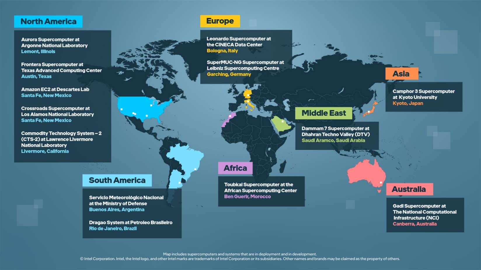
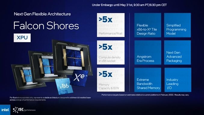
Intel Delivers AI-Accelerated HPC Performance

At the ISC High Performance Conference, Intel showcased leadership performance for high performance computing (HPC) and artificial intelligence (AI) workloads; shared its portfolio of future HPC and AI products, unified by the oneAPI open programming model; and announced an ambitious international effort to use the Aurora supercomputer to develop generative AI models for science and society.

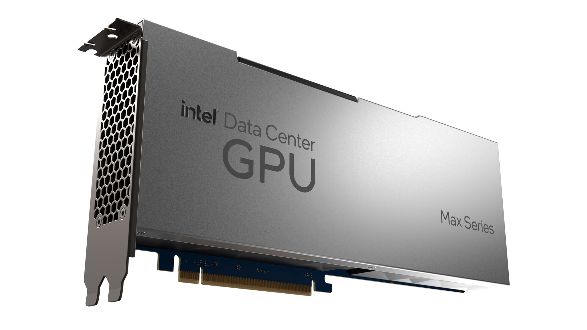
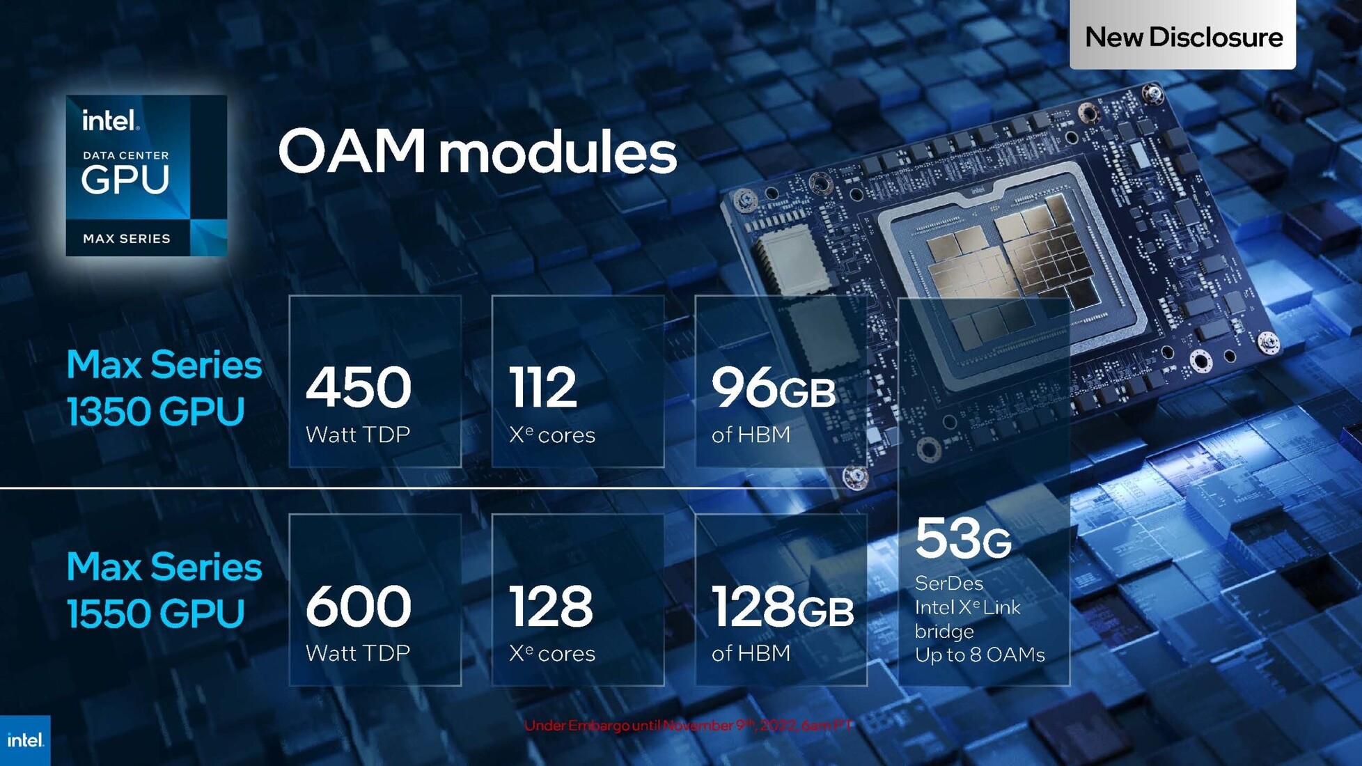
"Intel is committed to serving the HPC and AI community with products that help customers and end-users make breakthrough discoveries faster," said Jeff McVeigh, Intel corporate vice president and general manager of the Super Compute Group. "Our product portfolio spanning Intel Xeon CPU Max Series, Intel Data Center GPU Max Series, 4th Generation Intel Xeon Scalable Processors and Habana Gaudi 2 are outperforming the competition on a variety of workloads, offering energy and total cost of ownership advantages, democratizing AI and providing choice, openness and flexibility."

Intel Launches Agilex 7 FPGAs with R-Tile, First FPGA with PCIe 5.0 and CXL Capabilities

Intel's Programmable Solutions Group today announced that the Intel Agilex 7 with the R-Tile chiplet is shipping production-qualified devices in volume - bringing customers the first FPGA with PCIe 5.0 and CXL capabilities and the only FPGA with hard intellectual property (IP) supporting these interfaces. "Customers are demanding cutting-edge technology that offers the scalability and customization needed to not only efficiently manage current workloads, but also pivot capabilities and functions as their needs evolve. Our Agilex products offer the programmable innovation with the speed, power and capabilities our customers need while providing flexibility and resilience for the future. For example, customers are leveraging R-Tile, with PCIe Gen 5 and CXL, to accelerate software and data analytics, cutting the processing time from hours to minutes," said Shannon Poulin, Intel corporate vice president and general manager of the Programmable Solutions Group.

Faced with time, budget and power constraints, organizations across industries including data center, telecommunications and financial services, turn to FPGAs as flexible, programmable and efficient solutions. Using Agilex 7 with R-Tile, customers can seamlessly connect their FPGAs with processors, such as 4th Gen Intel Xeon Scalable processors, with the highest bandwidth processor interfaces to accelerate targeted data center and high performance computing (HPC) workloads. Agilex 7's configurable and scalable architecture enables customers to quickly deploy customized technology - at scale with hardware speeds based on their specific needs - to reduce overall design costs and development processes and to expedite execution to achieve optimal data center performance.

Frontier Remains As Sole Exaflop Machine on TOP500 List

Increasing its HPL score from 1.02 Eflop/s in November 2022 to an impressive 1.194 Eflop/s on this list, Frontier was able to improve upon its score after a stagnation between June 2022 and November 2022. Considering exascale was only a goal to aspire to just a few years ago, a roughly 17% increase here is an enormous success. Additionally, Frontier earned a score of 9.95 Eflop/s on the HLP-MxP benchmark, which measures performance for mixed-precision calculation. This is also an increase over the 7.94 EFlop/s that the system achieved on the previous list and nearly 10 times more powerful than the machine's HPL score. Frontier is based on the HPE Cray EX235a architecture and utilizes AMD EPYC 64C 2 GHz processors. It also has 8,699,904 cores and an incredible energy efficiency rating of 52.59 Gflops/watt. It also relies on gigabit ethernet for data transfer.

NVIDIA Grace Drives Wave of New Energy-Efficient Arm Supercomputers

NVIDIA today announced a supercomputer built on the NVIDIA Grace CPU Superchip, adding to a wave of new energy-efficient supercomputers based on the Arm Neoverse platform. The Isambard 3 supercomputer to be based at the Bristol & Bath Science Park, in the U.K., will feature 384 Arm-based NVIDIA Grace CPU Superchips to power medical and scientific research, and is expected to deliver 6x the performance and energy efficiency of Isambard 2, placing it among Europe's most energy-efficient systems.

It will achieve about 2.7 petaflops of FP64 peak performance and consume less than 270 kilowatts of power, ranking it among the world's three greenest non-accelerated supercomputers. The project is being led by the University of Bristol, as part of the research consortium the GW4 Alliance, together with the universities of Bath, Cardiff and Exeter.

Samsung Trademark Applications Hint at Next Gen DRAM for HPC & AI Platforms

The Korea Intellectual Property Rights Information Service (KIPRIS) has been processing a bunch of trademark applications in recent weeks, submitted by Samsung Electronics Corporation. News outlets pointed out, earlier on this month, that the South Korean multinational manufacturing conglomerate was attempting to secure the term "Snowbolt" as a moniker for an unreleased HBM3P DRAM-based product. Industry insiders and Samsung representatives have indicated that high bandwidth memory (5 TB/s bandwidth speeds per stack) will be featured in upcoming cloud servers, high-performance and AI computing - slated for release later on in 2023.

A Samsung-focused news outlet, SamMobile, has reported (on May 15) of further trademark applications for next generation DRAM (Dynamic Random Access Memory) products. Samsung has filed for two additional monikers - "Shinebolt" and "Flamebolt" - details published online show that these products share the same "designated goods" descriptors with the preceding "Snowbolt" registration: "DRAM modules with high bandwidth for use in high-performance computing equipment, artificial intelligence, and supercomputing equipment" and "DRAM with high bandwidth for use in graphic cards." Kye Hyun Kyung, CEO of Samsung Semiconductor, has been talking up his company's ambitions of competing with rival TSMC in providing cutting edge component technology, especially in the field of AI computing. It is too early to determine whether these "-bolt" DRAM products will be part of that competitive move, but it is good to know that speedier memory is on the way - future generation GPUs are set to benefit.

Samsung to Detail SF4X Process for High-Performance Chips

Samsung has invested heavily in semiconductor manufacturing technology to provide clients with a viable alternative to TSMC and its portfolio of nodes spanning anything from mobile to high-performance computing (HPC) applications. Today, we have information that Samsung will present its SF4X node to the public in this year's VLSI Symposium. Previously known as a 4HPC node, it is designed as a 4 nm-class node with a specialized use case for HPC processors, in contrast to the standard SF4 (4LPP) node that uses 4 nm transistors designed for low-power standards applicable to mobile/laptop space. According to the VLSI Symposium schedule, Samsung is set to present more info about the paper titled "Highly Reliable/Manufacturable 4nm FinFET Platform Technology (SF4X) for HPC Application with Dual-CPP/HP-HD Standard Cells."

As the brief introduction notes, "In this paper, the most upgraded 4nm (SF4X) ensuring HPC application was successfully demonstrated. Key features are (1) Significant performance +10% boosting with Power -23% reduction via advanced SD stress engineering, Transistor level DTCO (T-DTCO) and [middle-of-line] MOL scheme, (2) New HPC options: Ultra-Low-Vt device (ULVT), high speed SRAM and high Vdd operation guarantee with a newly developed MOL scheme. SF4X enhancement has been proved by a product to bring CPU Vmin reduction -60mV / IDDQ -10% variation reduction together with improved SRAM process margin. Moreover, to secure high Vdd operation, Contact-Gate breakdown voltage is improved by >1V without Performance degradation. This SF4X technology provides a tremendous performance benefits for various applications in a wide operation range." While we have no information on the reference for these claims, we suspect it is likely the regular SF4 node. More performance figures and an in-depth look will be available on Thursday, June 15, at Technology Session 16 at the symposium.

Nfina Technologies Releases Two New 3rd Gen Intel Xeon Scalable Processor-based Systems

Nfina announces the addition of two new server systems to its lineup, customized for small to medium businesses and virtualized environments. Featuring 3rd Gen Intel Xeon Scalable Processors, these scalable server systems fill a void in the marketplace, bringing exceptional multi-socket processing performance, easy setup, operability, and Nfina's five-year warranty.

"We are excited to add two new 3rd generation Intel systems to Nfina's lineup. Performance, scalability, and flexibility are key deciding factors when expanding our offerings," says Warren Nicholson, President and CEO of Nfina. "Both servers are optimized for high- performance computing, virtualized environments, and growing data needs." He continues by saying, "The two servers can also be leased through our managed services division. We provide customers with choices that fit the size of their application and budget - not a one size fits all approach."

Investment Firm KKR to Acquire CoolIT Systems for $270 Million

KKR, a leading global investment firm, and CoolIT Systems, a leading provider of scalable liquid cooling solutions for the world's most demanding computing environments, today announced the signing of a definitive agreement under which KKR will acquire CoolIT. The deal, valued at $270 million, will give CoolIT Systems added capital and other resources to scale up to meet growing demand for cooling systems from data-center operators, including giant cloud-computing providers such as Amazon.com's Amazon Web Services and Microsoft's Azure cloud unit. CoolIT also works with individual companies running AI applications and other business software in their own data centers.

Founded in 2001, CoolIT designs, engineers and manufactures advanced liquid cooling solutions for the data center and desktop markets. CoolIT's patented Split-Flow Direct Liquid Cooling technology is designed to improve equipment reliability and lifespan, decrease operating cost, lower energy demand and carbon emissions, reduce water consumption and allow for higher server density than legacy air-cooling methods.

"Our business has evolved tremendously over the past few years and today we are proud to be one of the most trusted providers of liquid cooling solutions to the global data center market," said Steve Walton, Chief Executive Officer of CoolIT. "KKR shares our perspective on the significant opportunity ahead for liquid cooling. Having access to KKR's expertise, capital and resources will put us in an even better position to keep scaling, innovating and delivering for our customers."

MIT Researchers Grow Transistors on Top of Silicon Wafers

MIT researchers have developed a groundbreaking technology that allows for the growth of 2D transition metal dichalcogenide (TMD) materials directly on fully fabricated silicon chips, enabling denser integrations. Conventional methods require temperatures of about 600°C, which can damage silicon transistors and circuits as they break down above 400°C. The MIT team overcame this challenge by creating a low-temperature growth process that preserves the chip's integrity, allowing 2D semiconductor transistors to be directly integrated on top of standard silicon circuits. The new approach grows a smooth, highly uniform layer across an entire 8-inch wafer, unlike previous methods that involved growing 2D materials elsewhere before transferring them to a chip or wafer. This process often led to imperfections that negatively impacted device and chip performance.

Additionally, the novel technology can grow a uniform layer of TMD material in less than an hour over 8-inch wafers, a significant improvement from previous methods that required over a day for a single layer. The enhanced speed and uniformity of this technology make it suitable for commercial applications, where 8-inch or larger wafers are essential. The researchers focused on molybdenum disulfide, a flexible, transparent 2D material with powerful electronic and photonic properties ideal for semiconductor transistors. They designed a new furnace for the metal-organic chemical vapor deposition process, which has separate low and high-temperature regions. The silicon wafer is placed in the low-temperature region while vaporized molybdenum and sulfur precursors flow into the furnace. Molybdenum remains in the low-temperature region, while the sulfur precursor decomposes in the high-temperature region before flowing back into the low-temperature region to grow molybdenum disulfide on the wafer surface.

Samsung Electronics Announces First Quarter 2023 Results, Profits Lowest in 14 Years

Samsung Electronics today reported financial results for the first quarter ended March 31, 2023. The Company posted KRW 63.75 trillion in consolidated revenue, a 10% decline from the previous quarter, as overall consumer spending slowed amid the uncertain global macroeconomic environment. Operating profit was KRW 0.64 trillion as the DS (Device Solutions) Division faced decreased demand, while profit in the DX (Device eXperience) Division increased.

The DS Division's profit declined from the previous quarter due to weak demand in the Memory Business, a decline in utilization rates in the Foundry Business and continued weak demand and inventory adjustments from customers. Samsung Display Corporation (SDC) saw earnings in the mobile panel business decline quarter-on-quarter amid a market contraction, while the large panel business slightly narrowed its losses. The DX Division's results improved on the back of strong sales of the premium Galaxy S23 series as well as an enhanced sales mix focusing on premium TVs.

TSMC Showcases New Technology Developments at 2023 Technology Symposium

TSMC today showcased its latest technology developments at its 2023 North America Technology Symposium, including progress in 2 nm technology and new members of its industry-leading 3 nm technology family, offering a range of processes tuned to meet diverse customer demands. These include N3P, an enhanced 3 nm process for better power, performance and density, N3X, a process tailored for high performance computing (HPC) applications, and N3AE, enabling early start of automotive applications on the most advanced silicon technology.

With more than 1,600 customers and partners registered to attend, the North America Technology Symposium in Santa Clara, California is the first of the TSMC's Technology Symposiums around the world in the coming months. The North America symposium also features an Innovation Zone spotlighting the exciting technologies of 18 emerging start-up customers.

Samsung Hit With $303 Million Fine, Sued Over Alleged Memory Patent Infringements

Netlist Inc. an enterprise solid state storage drive specialist has been awarded over $303 million in damages by a federal jury in Texas on April 21, over apparent patent infringement on Samsung's part. Netlist has alleged that the South Korean multinational electronics corporation had knowingly infringed on five patents, all relating to improvements in data processing within the design makeup of memory modules intended for high performance computing (HPC) purposes. The Irvine, CA-based computer-memory specialist has sued Samsung in the past - with a legal suit filed at the Federal District Court for the Central District of California.

Netlist was seemingly pleased by the verdict reached at the time (2021) when the court: "granted summary judgements in favor of Netlist and against Samsung for material breach of various obligations under the Joint Development and License Agreement (JDLA), which the parties executed in November 2015. A summary judgment is a final determination rendered by the judge and has the same force and effect as a final ruling after a jury trial in litigation."

SK hynix Develops Industry's First 12-Layer HBM3, Provides Samples To Customers

SK hynix announced today it has become the industry's first to develop 12-layer HBM3 product with a 24 gigabyte (GB) memory capacity, currently the largest in the industry, and said customers' performance evaluation of samples is underway. HBM (High Bandwidth Memory): A high-value, high-performance memory that vertically interconnects multiple DRAM chips and dramatically increases data processing speed in comparison to traditional DRAM products. HBM3 is the 4th generation product, succeeding the previous generations HBM, HBM2 and HBM2E

"The company succeeded in developing the 24 GB package product that increased the memory capacity by 50% from the previous product, following the mass production of the world's first HBM3 in June last year," SK hynix said. "We will be able to supply the new products to the market from the second half of the year, in line with growing demand for premium memory products driven by the AI-powered chatbot industry." SK hynix engineers improved process efficiency and performance stability by applying Advanced Mass Reflow Molded Underfill (MR-MUF)# technology to the latest product, while Through Silicon Via (TSV)## technology reduced the thickness of a single DRAM chip by 40%, achieving the same stack height level as the 16 GB product.

AMD Joins AWS ISV Accelerate Program

AMD announced it has joined the Amazon Web Services (AWS) Independent Software Vendor (ISV) Accelerate Program, a co-sell program for AWS Partners - like AMD - who provide integrated solutions on AWS. The program helps AWS Partners drive new business by directly connecting participating ISVs with the AWS Sales organization.

Through the AWS ISV Accelerate Program, AMD will receive focused co-selling support from AWS, including, access to further sales enablement resources, reduced AWS Marketplace listing fees, and incentives for AWS Sales teams. The program will also allow participating ISVs access to millions of active AWS customers globally.

Bulk Order of GPUs Points to Twitter Tapping Big Time into AI Potential

According to Business Insider, Twitter has made a substantial investment into hardware upgrades at its North American datacenter operation. The company has purchased somewhere in the region of 10,000 GPUs - destined for the social media giant's two remaining datacenter locations. Insider sources claim that Elon Musk has committed to a large language model (LLM) project, in an effort to rival OpenAI's ChatGPT system. The GPUs will not provide much computational value in the current/normal day-to-day tasks at Twitter - the source reckons that the extra processing power will be utilized for deep learning purposes.

Twitter has not revealed any concrete plans for its relatively new in-house artificial intelligence project but something was afoot when, earlier this year, Musk recruited several research personnel from Alphabet's DeepMind division. It was theorized that he was incubating a resident AI research lab at the time, following personal criticisms levelled at his former colleagues at OpenAI, ergo their very popular and much adopted chatbot.

Intel Discontinues Brand New Max 1350 Data Center GPU, Successor Targets Alternative Markets

Intel has decided to re-organize its Max series of Data Center GPUs (codenamed Ponte Vecchio), as revealed to Tom's Hardware this week, with a particular model - the Data Center Max GPU 1350 set for removal from the lineup. Industry experts are puzzled by this decision, given that the 1350 has been officially "available" on the market since January 2023, following soon after the announcement of the entire Max range in November 2022. Intel has removed listings and entries for the Data Center GPU Max 1350 from its various web presences.

A (sort of) successor is in the works, Intel has lined up the Data Center Max GPU 1450 for release later in the year. This model will have a trimmed I/O bandwidth - this modification is likely targeting companies in China, where performance standards are capped at a certain level (via U.S. sanctions on GPU exports). An Intel spokesperson provided further details and reasons for rearranging the Max product range: "We launched the Intel Data Center Max GPU 1550 (600 W), which was initially targeted for liquid-cooled solutions only. We have since expanded our support by offering Intel Data Center Max GPU 1550 (600 W) to include air-cooled solutions."

Chinese GPU Maker Biren Technology Loses its Co-Founder, Only Months After Revealing New GPUs

Golf Jiao, a co-founder and general manager of Biren Technology, has left the company late last month according to insider sources in China. No official statement has been issued by the executive team at Biren Tech, and Jiao has not provided any details regarding his departure from the fabless semiconductor design company. The Shanghai-based firm is a relatively new startup - it was founded in 2019 by several former NVIDIA, Qualcomm and Alibaba veterans. Biren Tech received $726.6 million in funding for its debut range of general-purpose graphics processing units (GPGPUs), also defined as high-performance computing graphics processing units (HPC GPUs).

The company revealed its ambitions to take on NVIDIA's Ampere A100 and Hopper H100 compute platforms, and last August announced two HPC GPUs in the form of the BR100 and BR104. The specifications and performance charts demonstrated impressive figures, but Biren Tech had to roll back its numbers when it was hit by U.S Government enforced sanctions in October 2022. The fabless company had contracted with TSMC to produce its Biren range, and the new set of rules resulted in shipments from the Taiwanese foundry being halted. Biren Tech cut its work force by a third soon after losing its supply chain with TSMC, and the engineering team had to reassess how the BR100 and BR104 would perform on a process node larger than the original 7 nm design. It was decided that a downgrade in transfer rates would appease the legal teams, and get newly redesigned Biren silicon back onto the assembly line.

NVIDIA Executive Says Cryptocurrencies Add Nothing Useful to Society

In an interview with The Guardian, NVIDIA's Chief Technical Officer (CTO) Michael Kagan added his remarks on the company and its cryptocurrency position. Being the maker of the world's most powerful graphics cards and compute accelerators, NVIDIA is the most prominent player in the industry regarding any computing application from cryptocurrencies to AI and HPC. In the interview, Mr. Kegan expressed his opinions and argued that newly found applications such as ChatGTP bring much higher value to society compared to cryptocurrencies. "All this crypto stuff, it needed parallel processing, and [Nvidia] is the best, so people just programmed it to use for this purpose. They bought a lot of stuff, and then eventually it collapsed, because it doesn't bring anything useful for society. AI does," said Kegan, adding that "I never believed that [crypto] is something that will do something good for humanity. You know, people do crazy things, but they buy your stuff, you sell them stuff. But you don't redirect the company to support whatever it is."

When it comes to AI and other applications, the company has a very different position. "With ChatGPT, everybody can now create his own machine, his own programme: you just tell it what to do, and it will. And if it doesn't work the way you want it to, you tell it 'I want something different," he added, arguing that the new AI applications have usability level beyond that of crypto. Interestingly, trading applications are also familiar to NVIDIA, as they had clients (banks) using their hardware for faster trading execution. Mr. Kegan noted: "We were heavily involved in also trading: people on Wall Street were buying our stuff to save a few nanoseconds on the wire, the banks were doing crazy things like pulling the fibers under the Hudson taut to make them a little bit shorter, to save a few nanoseconds between their datacentre and the stock exchange."

Supermicro Expands GPU Solutions Portfolio with Deskside Liquid-Cooled AI Development Platform, Powered by NVIDIA

Supermicro, Inc., a Total IT Solution Provider for Cloud, AI/ML, Storage, and 5G/Edge, is announcing the first in a line of powerful yet quiet and power-efficient NVIDIA-accelerated AI Development platforms which gives information professionals and developers the most powerful technology available today at their deskside. The new AI development platform, the SYS-751GE-TNRT-NV1, is an application-optimized system that excels when developing and running AI-based software. This innovative system gives developers and users a complete HPC and AI resource for department workloads. In addition, this powerful system can support a small team of users running training, inference, and analytics workloads simultaneously.

The self-contained liquid-cooling feature addresses the thermal design power needs of the four NVIDIA A100 Tensor Core GPUs and the two 4th Gen Intel Xeon Scalable CPUs to enable full performance while improving the overall system's efficiency and enabling quiet (approximately 30dB) operation in an office environment. In addition, this system is designed to accommodate high-performing CPUs and GPUs, making it ideal for AI/DL/ML and HPC applications. The system can reside in an office environment or be rack-mounted when installed in a data center environment, simplifying IT management.

ASUS Announces NVIDIA-Certified Servers and ProArt Studiobook Pro 16 OLED at GTC

ASUS today announced its participation in NVIDIA GTC, a developer conference for the era of AI and the metaverse. ASUS will offer comprehensive NVIDIA-certified server solutions that support the latest NVIDIA L4 Tensor Core GPU—which accelerates real-time video AI and generative AI—as well as the NVIDIA BlueField -3 DPU, igniting unprecedented innovation for supercomputing infrastructure. ASUS will also launch the new ProArt Studiobook Pro 16 OLED laptop with the NVIDIA RTX 3000 Ada Generation Laptop GPU for mobile creative professionals.

Purpose-built GPU servers for generative AI
Generative AI applications enable businesses to develop better products and services, and deliver original content tailored to the unique needs of customers and audiences. ASUS ESC8000 and ESC4000 are fully certified NVIDIA servers that support up to eight NVIDIA L4 Tensor Core GPUs, which deliver universal acceleration and energy efficiency for AI with up to 2.7X more generative AI performance than the previous GPU generation. ASUS ESC and RS series servers are engineered for HPC workloads, with support for the NVIDIA Bluefield-3 DPU to transform data center infrastructure, as well as NVIDIA AI Enterprise applications for streamlined AI workflows and deployment.

Supermicro Servers Now Featuring NVIDIA HGX and PCIe-Based H100 8-GPU Systems

Supermicro, Inc., a Total IT Solution Provider for AI/ML, Cloud, Storage, and 5G/Edge, today has announced that it has begun shipping its top-of-the-line new GPU servers that feature the latest NVIDIA HGX H100 8-GPU system. Supermicro servers incorporate the new NVIDIA L4 Tensor Core GPU in a wide range of application-optimized servers from the edge to the data center.

"Supermicro offers the most comprehensive portfolio of GPU systems in the industry, including servers in 8U, 6U, 5U, 4U, 2U, and 1U form factors, as well as workstations and SuperBlade systems that support the full range of new NVIDIA H100 GPUs," said Charles Liang, president and CEO of Supermicro. "With our new NVIDIA HGX H100 Delta-Next server, customers can expect 9x performance gains compared to the previous generation for AI training applications. Our GPU servers have innovative airflow designs which reduce fan speeds, lower noise levels, and consume less power, resulting in a reduced total cost of ownership (TCO). In addition, we deliver complete rack-scale liquid-cooling options for customers looking to further future-proof their data centers."

NVIDIA to Lose Two Major HPC Partners in China, Focuses on Complying with Export Control Rules

NVIDIA's presence in high-performance computing has steadily increased, with various workloads benefiting from the company's AI and HPC accelerator GPUs. One of the important markets for the company is China, and export regulations are about to complicate NVIDIA's business dealing with the country. NVIDIA's major partners in the Asia Pacific region are Inspur and Huawei, which make servers powered by A100 and H100 GPU solutions. Amid the latest Biden Administration complications, the US is considering limiting more export of US-designed goods to Chinese entities. Back in 2019, the US blacklisted Huawei and restricted the sales of the latest GPU hardware to the company. Last week, the Biden Administration also blacklisted Inspur, the world's third-largest server maker.

In the Morgan Stanley conference, NVIDIA's Chief Financial Officer Colette Cress noted that: "Inspur is a partner for us, when we indicate a partner, they are helping us stand up computing for the end customers. As we work forward, we will probably be working with other partners, for them to stand-up compute within the Asia-Pac region or even other parts of the world. But again, our most important focus is focusing on the law and making sure that we follow export controls very closely. So in this case, we will look in terms of other partners to help us." This indicates that NVIDIA will lose millions of dollars in revenue due to the inability to sell its GPUs to partners like Inspur. As the company stated, complying with the export regulations is the most crucial focus.

Intel's Ponte Vecchio HPC GPU Successor Rialto Bridge Gets the Axe

Late on Friday in a newsroom posting by Intel's Interim GM Jeff McVeigh a roadmap uplift was quietly revealed. Rialto Bridge, the process improved version of Ponte Vecchio currently shipping under the Max Series GPU branding, has been pulled from the roadmap in favor of doubling down on the future design code-named Falcon Shores. Rialto Bridge was first announced last May at SC22 as the direct successor to Ponte Vecchio, and was set to begin sampling later this year. In the same post Intel also cancelled Lancaster Sound, their Visual Cloud GPU meant to replace the Arctic Sound Flex series of GPUs based on similar Xe cores to Arc Alchemist. In its stead the follow-up architecture Melville Sound will receive focused development efforts.

Falcon Shores is described as a new foundational chiplet architecture that will integrate more diverse compute tiles, creating what Intel originally dubbed the XPU. This next architectural step would combine what Intel is already doing with products such as Sapphire Rapids and Ponte Vecchio into one CPU+GPU package, and would offer even further flexibility to add other kinds of accelerators. With this roadmap update there is some uncertainty as to whether the XPU designation will make the transition as it is notably absent in the letter. It is clear though that Falcon Shores will directly replace Ponte Vecchio as the next HPC GPU, with or without CPU tiles included.

Revenue from Enterprise SSDs Totaled Just US$3.79 Billion for 4Q22 Due to Slumping Demand and Widening Decline in SSD Contract Prices, Says TrendForce

Looking back at 2H22, as server OEMs slowed down the momentum of their product shipments, Chinese server buyers also held a conservative outlook on future demand and focused on inventory reduction. Thus, the flow of orders for enterprise SSDs remained sluggish. However, NAND Flash suppliers had to step up shipments of enterprise SSDs during 2H22 because the demand for storage components equipped in notebook (laptop) computers and smartphones had undergone very large downward corrections. Compared with other categories of NAND Flash products, enterprise SSDs represented the only significant source of bit consumption. Ultimately, due to the imbalance between supply and demand, the QoQ decline in prices of enterprise SSDs widened to 25% for 4Q22. This price plunge, in turn, caused the quarterly total revenue from enterprise SSDs to drop by 27.4% QoQ to around US$3.79 billion. TrendForce projects that the NAND Flash industry will again post a QoQ decline in the revenue from this product category for 1Q23.

Ayar Labs Demonstrates Industry's First 4-Tbps Optical Solution, Paving Way for Next-Generation AI and Data Center Designs

Ayar Labs, a leader in the use of silicon photonics for chip-to-chip optical connectivity, today announced public demonstration of the industry's first 4 terabit-per-second (Tbps) bidirectional Wavelength Division Multiplexing (WDM) optical solution at the upcoming Optical Fiber Communication Conference (OFC) in San Diego on March 5-9, 2023. The company achieves this latest milestone as it works with leading high-volume manufacturing and supply partners including GlobalFoundries, Lumentum, Macom, Sivers Photonics and others to deliver the optical interconnects needed for data-intensive applications. Separately, the company was featured in an announcement with partner Quantifi Photonics on a CW-WDM-compliant test platform for its SuperNova light source, also at OFC.

In-package optical I/O uniquely changes the power and performance trajectories of system design by enabling compute, memory and network silicon to communicate with a fraction of the power and dramatically improved performance, latency and reach versus existing electrical I/O solutions. Delivered in a compact, co-packaged CMOS chiplet, optical I/O becomes foundational to next-generation AI, disaggregated data centers, dense 6G telecommunications systems, phased array sensory systems and more.
Return to Keyword Browsing
May 21st, 2024 09:11 EDT change timezone

New Forum Posts

Popular Reviews

Controversial News Posts