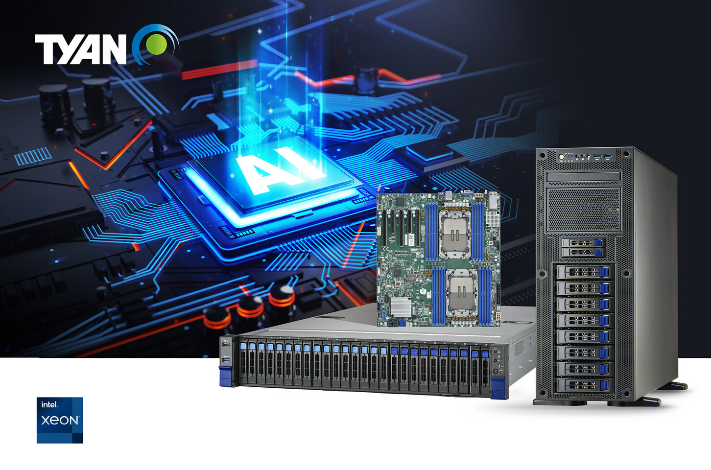
GIGABYTE Enterprise Servers & Motherboards Roll Out on European E-commerce Platform
GIGABYTE Technology, a pioneer in computer hardware, has taken a significant stride in shaping its European business model. Today, GIGABYTE has broadened its e-commerce platform, shop.gigabyte.eu, by integrating enterprise server and server motherboard solutions into its product portfolio. Being at the forefront of computer hardware manufacturing, GIGABYTE recognizes that it is imperative to expand its presence in the EMEA region to maintain its leadership across all markets. With the introduction of our enterprise-level server and motherboard solutions, we are dedicated to delivering a diverse range of high-performance products directly to our B2B clients.
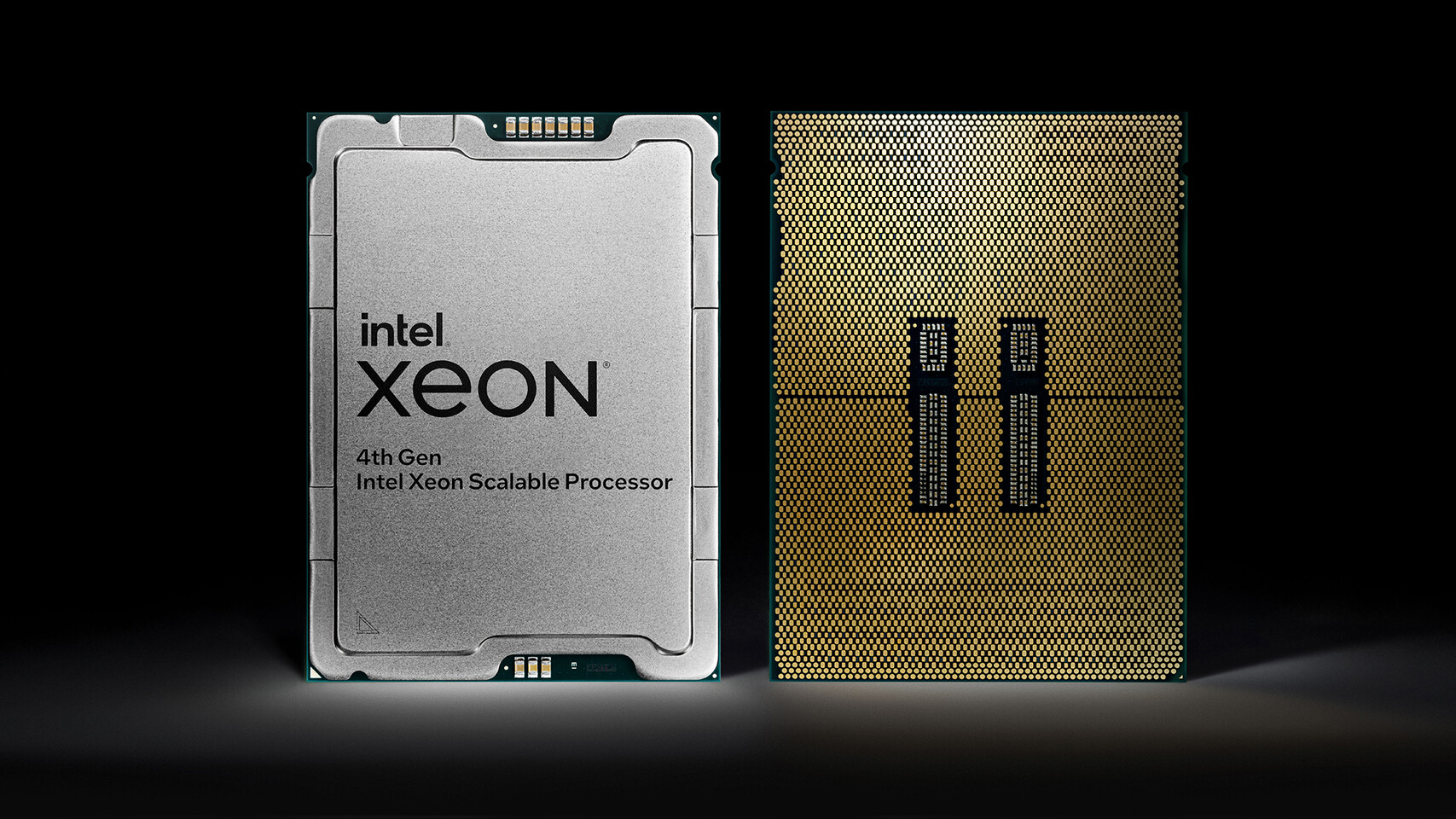
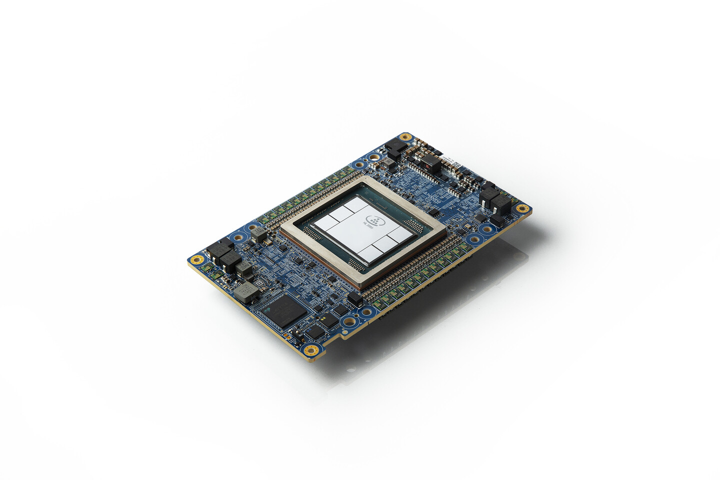
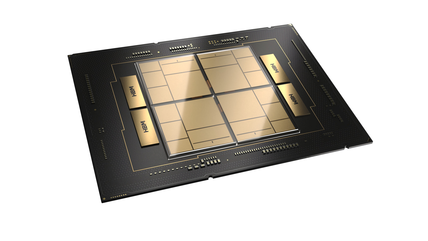
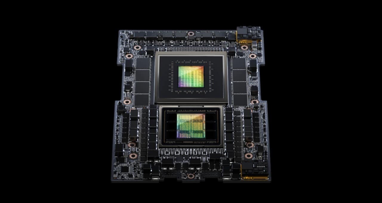
GIGABYTE offers a complete product portfolio that addresses all workloads from the data center to edge including traditional and emerging workloads in HPC and AI to data analytics, 5G/edge, cloud computing, and more. Our enduring partnerships with key technology leaders ensure that our new products are at the forefront of innovation and launch with new partner platforms. Our systems embody performance, security, scalability, and sustainability. Within the e-commerce product portfolio, we offer a selection of models from our Edge, Rack, GPU, and Storage series. Additionally, the platform provides server motherboards for custom integration. The current selection comprises a mix of solutions tailored to online sales. For more complex solutions, customers can get in touch via the integrated contact form.
GIGABYTE offers a complete product portfolio that addresses all workloads from the data center to edge including traditional and emerging workloads in HPC and AI to data analytics, 5G/edge, cloud computing, and more. Our enduring partnerships with key technology leaders ensure that our new products are at the forefront of innovation and launch with new partner platforms. Our systems embody performance, security, scalability, and sustainability. Within the e-commerce product portfolio, we offer a selection of models from our Edge, Rack, GPU, and Storage series. Additionally, the platform provides server motherboards for custom integration. The current selection comprises a mix of solutions tailored to online sales. For more complex solutions, customers can get in touch via the integrated contact form.