News Posts matching #IP

Return to Keyword Browsing

Marvell and AWS Collaborate to Enable Cloud-First Silicon Design

Marvell Technology, Inc., a leader in data infrastructure semiconductor solutions, announced today that it has selected Amazon Web Services, Inc. (AWS) as its cloud provider for electronic design automation (EDA). A cloud-first approach helps Marvell to rapidly and securely scale its service on the world's leading cloud, rise to the challenges brought by increasingly complex chip design processes, and deliver continuous innovation for the expanding needs across the automotive, carrier, data center, and enterprise infrastructure markets it serves. The work extends the longstanding relationship between the two companies—Marvell is also a key semiconductor supplier for AWS, helping the company support the design and rapid delivery of cloud services that best meet customers' demanding requirements.

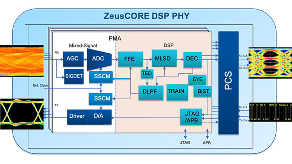
EDA refers to the specialized and compute-intensive processes used in chip making and is a critical piece of Marvell's R&D. Over the years, the number of transistors on an integrated chip has increased exponentially. Each advance in chip design calls for a calculated application of software modules overseeing logic design, debugging, component placement, wire routing, optimization of time and power consumption, and verification. Due to the computationally intensive nature of EDA workloads, it is no longer cost-effective or timely to run EDA on premises. By powering its EDA with AWS, Marvell leverages an unmatched portfolio of services including secure, elastic, high-performance compute capacity in the cloud to solve challenges around speed, latency, security of IP, and data transfer.

Intel Slashes Dividend By Two-Thirds, Updates Capital Allocation

Intel Corporation today announced that its board of directors has reset its dividend policy, reducing the quarterly dividend to $0.125 per share (or $0.50 annually) on the company's common stock. The dividend will be payable on June 1, 2023, to stockholders of record on May 7, 2023. Intel also reaffirmed its first-quarter 2023 business outlook provided at its most recent earnings call, including revenue of between $10.5 billion and $11.5 billion; gross margin of 34.1% on a GAAP basis and 39% on a non-GAAP basis; tax rate of (84%) on a GAAP basis and 13% on a non-GAAP basis; and earnings per share of $(0.80) on a GAAP basis and $(0.15) on a non-GAAP basis.

The decision to decrease the quarterly dividend reflects the board's deliberate approach to capital allocation and is designed to best position the company to create long-term value. The improved financial flexibility will support the critical investments needed to execute Intel's transformation during this period of macroeconomic uncertainty. Since first initiated in 1992, Intel's dividend has delivered more than $80 billion in cash returns to the company's stockholders, and the board is committed to maintaining a competitive dividend.

ASML's Ex-Employee in China Allegedly Stole Confidential Information

The Netherlands-based ASML has reportedly launched a comprehensive investigation into the company's branch in China following reports that one of its former employees allegedly stole confidential information. According to Bloomberg, the employee in question was part of a product life cycle management (PLM) program for ASML's advanced lithography solutions. Specifically, the employee worked for the Teamcenter software division responsible for lithography tool management. This software was used to create digital twins of scanners and other tools and allowed information to be shared among the company's employees. In ASML's case, the software contained all the confidential information about the scanners and how they work, which makes it a target for IP theft. We do not know if this is a China-sponsored action to boost its domestic lithography tool development; however, ASML has issued a statement below.
ASMLWe have experienced unauthorized misappropriation of data relating to proprietary technology by a (now) former employee in China. We promptly initiated a comprehensive internal review. Based upon our initial findings we do not believe that the misappropriation is material to our business. However, as a result of the security incident, certain export control regulations may have been violated. ASML has therefore reported the incident to relevant authorities. We are implementing additional remedial measures in light of this incident.

League of Legends Source Code Stolen in Riot Games Cyberattack

Riot Games provided its first response to last week's cyberattack on its company network. The company alleges that the attackers have exfiltrated with the source-codes for "League of Legends," "Teamfight Tactics," and a proprietary anti-cheat software that's no longer in use. Riot Games assures all that no game user data was compromised with this attack (particularly passwords or payment-instrument details); and at worst the stolen source code could help the attackers create cheats. The company also received a ransom e-mail from the attackers demanding payment, failing which they threaten to release the source code to public; but Riot said that it does not intend to pay. Since user information isn't compromised, and the games themselves are protected by IP laws globally, there's little reason to pay up.

AMD Shows Instinct MI300 Exascale APU with 146 Billion Transistors

During its CES 2023 keynote, AMD announced its latest Instinct MI300 APU, a first of its kind in the data center world. Combining the CPU, GPU, and memory elements into a single package eliminates latency imposed by long travel distances of data from CPU to memory and from CPU to GPU throughout the PCIe connector. In addition to solving some latency issues, less power is needed to move the data and provide greater efficiency. The Instinct MI300 features 24 Zen4 cores with simultaneous multi-threading enabled, CDNA3 GPU IP, and 128 GB of HBM3 memory on a single package. The memory bus is 8192-bit wide, providing unified memory access for CPU and GPU cores. CLX 3.0 is also supported, making cache-coherent interconnecting a reality.

The Instinct MI300 APU package is an engineering marvel of its own, with advanced chiplet techniques used. AMD managed to do 3D stacking and has nine 5 nm logic chiplets that are 3D stacked on top of four 6 nm chiplets with HBM surrounding it. All of this makes the transistor count go up to 146 billion, representing the sheer complexity of a such design. For performance figures, AMD provided a comparison to Instinct MI250X GPU. In raw AI performance, the MI300 features an 8x improvement over MI250X, while the performance-per-watt is "reduced" to a 5x increase. While we do not know what benchmark applications were used, there is a probability that some standard benchmarks like MLPerf were used. For availability, AMD targets the end of 2023, when the "El Capitan" exascale supercomputer will arrive using these Instinct MI300 APU accelerators. Pricing is unknown and will be unveiled to enterprise customers first around launch.

Achronix Announces Speedster7t AC7t1500 FPGA General Availability

In a continuing commitment to enabling industry-leading data acceleration in heterogeneous compute environments, Achronix Semiconductor Corporation, the industry's only independent supplier of high-end FPGAs and eFPGA IP solutions, today announced the production release of its AC7t1500 FPGA and the addition of the power-efficient AC7t800 FPGA to the Achronix Tool Suite.

"The Speedster 7t product family offers unprecedented FPGA-based performance for data acceleration applications," said Steve Mensor, VP of Marketing and Business Development at Achronix. "The release of the AC7t1500 to production along with the addition of the AC7t800 in our ACE design tools gives customers multiple options from this industry-leading, high-performance family that offers FPGA programmability with ASIC-level performance. These advancements give customers confidence that they can design on a robust, validated FPGA product family that meets their high-performance and high-bandwidth needs."

Export Regulations Hinder China's Plans for Custom Arm-Based Processors

The United States has recently imposed several sanctions on technology exports to China. These sanctions are designed to restrict the transfer of specific technologies and sensitive information to Chinese entities, particularly those with ties to the Chinese military or government. The primary motivation behind these sanctions is to protect American national security interests, as well as to protect American companies from unfair competition. According to Financial Times, we have information that Chinese tech Giant, Alibaba, can not access Arm licenses for Neoverse V1 technology. Generally, the technology group where Neoverse V-series falls in is called Wassenaar -- multilateral export control regime (MECR) with 42 participating states. This agreement prohibits the sale of technology that could be used for military purposes.

The US argues that Arm's Neoverse V1 IP is not only a product from UK's Arm but a design made in the US as well, meaning that it is a US technology. Since Alibaba's T-Head group responsible for designing processors that go into Alibaba's cloud services can not use Neoverse V1, it has to look for alternative solutions. The Neoverse V1 and V2 can not be sold in China, while Neoverse N1 and N2 can. Alibaba's T-Head engineer argued, "We feel that the western world sees us as second-class people. They won't sell good products to us even if we have money."

Lattice Extends Low Power Leadership with New Lattice Avant FPGA Platform

Lattice Semiconductor, the low power programmable leader, today unveiled Lattice Avant, a new FPGA platform purpose-built to bring the company's power efficient architecture, small size, and performance leadership to mid-range FPGAs. Lattice Avant offers best-in-class power efficiency, advanced connectivity, and optimized compute that enable Lattice to address an expanded set of customer applications across the Communications, Computing, Industrial, and Automotive markets.

"With Lattice Avant, we extend our low power leadership position in the FPGA industry and are poised to continue our rapid pace of innovation, while also doubling the addressable market for our product portfolio," said Jim Anderson, President and CEO, Lattice Semiconductor. "We created Avant to address our customers' need for compelling mid-range FPGA solutions, and we're excited to help them accelerate their designs with new levels of power efficiency and performance."

Arm Could Change Licensing Model to Charge OEMs Directly

Over the past few weeks, the legal dispute between Arm Ltd. and Qualcomm Inc. has been warming up the eyes of the entire tech community. However, as per the latest court filing, Arm could change its licensing strategy and shift its whole business model into a new direction that would benefit the company directly. Currently, the company provides the intellectual property (IP) that chip makers can use and add to designs mixed with other IPs and custom in-house solutions. That is how the world of electronics design (EDA) works and how many companies operate. However, in the Qualcomm-Arm legal battle, Qualcomm's counterclaim has brought new light about Arm's plans for licensing its hardware designs past 2024.

According to Dylan Patel of SemiAnalysis, who examined court documents, Arm will reportedly change terms to use its IP where the use of other IP mixed with Arm IP is prohibited. If a chip maker plans to use Arm CPU IP, they must also use Arm's GPU/NPU/ISP/DSP IPs. This would result in devices that utilize every design the UK-based designer has to offer, and other IP makers will have to exclude their designs from the SoC. By doing this, Arm directly stands against deals like the Samsung-AMD deal, where AMD provides RDNA GPU IP and would force Samsung to use Arm's Mali GPU IP instead. This change should take effect in 2025 when every new license agreement has to comply with new rules.

Alphawave IP Achieves Its First Testchip Tapeout for TSMC N3E Process

Alphawave IP (LSE: AWE), a global leader in high-speed connectivity for the world's technology infrastructure, today announced the successful tapeout of its ZeusCORE100 1-112 Gbps NRZ/PAM4 Serialiser-Deserialiser ("SerDes"), Alphawave's first testchip on TSMC's most advanced N3E process. Alphawave IP will be exhibiting this new product alongside its complete portfolio of high-performance IP, chiplet, and custom silicon solutions at the TSMC OIP Forum on October 26 in Santa Clara, CA as the Platinum sponsor.

ZeusCORE100 is Alphawave's most advanced multi-standard-SerDes, supporting extra-long channels over 45dB and the most requested standards such as 800G Ethernet, OIF 112G-CEI, PCIe GEN6, and CXL 3.0. Attendees will be able to visit the Alphawave booth and meet the company's technology experts including members of the recently acquired OpenFive team. OpenFive is a longstanding partner of TSMC through the OIP Value Chain Aggregator (VCA) program. OpenFive is one of a select few companies with an idea-to-silicon methodology in TSMC's latest technologies, and advanced packaging capabilities, enabling access to the most advanced foundry solution available with the best Power-Performance-Area (PPA). With Alphawave's industry-leading IP portfolio and the addition of OpenFive's capabilities, designers can create systems on a chip (SoCs) that pack more compute power into smaller form factors for networking, AI, storage, and high-performance computing (HPC) applications.

GIGABYTE Unveils Enterprise-grade Motherboards and an Entry Level Workstation for the Launch of AMD Ryzen 7000 Series

GIGABYTE Technology, (TWSE: 2376), an industry leader in high-performance servers and workstations, today announced supporting products for the new AMD AM5 platform starting with two GIGABYTE motherboards, MC13-LE0 & MC13-LE1, that pair a consumer CPU with IPMI management functionalities via BMC. Additionally, a new desktop workstation, W332-Z00, was released using the same motherboard series platform that supports remote management, but the W332 does so with a Realtek NIC that enables DASH.

The new GIGABYTE products designed to support host systems are deceivingly powerful with a small micro-ATX form factor motherboard and enterprise rich out-of-band management features on top of PCIe Gen 5 and DDR5 technologies. These new client friendly products will be found in office settings under a desk rather than a rack in a data center, as they be managed from anywhere, provided there is a network connection. Furthermore, these new products are purpose built for the mainstream AMD B650E chipset with AMD Zen 4 architecture for AMD Ryzen 7000 Series desktop processors.

Microsoft's Activision-Blizzard Acquisition Hits UK and EU Regulatory Hurdles

Microsoft's USD $68.7 billion acquisition of Activision-Blizzard is running into hurdles with competition regulators in both the UK and the EU, with both Brussels and London hinting at a thorough investigation into the impact the acquisition will have on competition in their respective markets. Microsoft is already a game publisher under Microsoft Games Studio, and makes at least two leading gaming platforms—the Xbox and Windows PC; whereas Activision-Blizzard own a constellation of dozens of game developers, and a mountain of IP over some of the most valuable game franchises of all time.

Britain's Competition and Markets Authority has hinted that the acquisition warrants a "second-phase investigation" since it has concerns that the deal would "result in a substantial lessening of competition within a market or markets in the United Kingdom." Over in Brussels, the EU market regulators, too, are taking a closer look at what the deal could entail for European consumers. Sony Computer Entertainment is particularly unhappy with the acquisition, and is the primary source of opposition to the deal that's invoked by regulators. Sony fears that with this acquisition, Microsoft will be in a position to deny popular game franchises such as "Call of Duty" to the PlayStation platform, and will have too much control over whether Sony can deliver an experience comparable or better than that of the Xbox.
Many Thanks to DeathtoGnomes for the tip.

Report: Apple to Move a Part of its Embedded Cores to RISC-V, Stepping Away from Arm ISA

According to Dylan Patel of SemiAnalysis sources, Apple is moving its embedded cores from Arm to RISC-V. In Apple's Silicon designs, there are far more cores than the main ones that power the operating system and end-user applications. For example, embedded cores are present, and there are 30+ in M1 SoCs responsible for all kinds of workloads not related to the operating system. These tasks are usually associated with other functions such as WiFi/BlueTooth, ThunderBolt retiming, touchpad control, NAND chips having their own core, etc. They run their own firmware and power everything around the central cores that run the OS, so the whole SoC functions appropriately.

It appears that a lot of these cores are based on Arm M-series or lower-end A-series IP that Apple is currently looking to replace with RISC-V. Given that a large portion of software runs on the main big.LITTLE configuration, other secondary SoC tasks can migrate to a different ISA like RISC-V, with a small firmware adjustment. Given that these cores can be placed with custom IPs, Apple would save licensing fees if custom RISC-V cores were used. Additionally, developing firmware for these cores at an Apple engineering team size shouldn't be a problem. Of course, we have no information about when these custom cores will appear inside Apple Silicon. Even when they are used, no formal announcement is expected given that the main cores remain to be powered by Arm ISA, with everything else invisible to the end-user.

Arm Announces Next-Generation Neoverse Cores for High Performance Computing

The demand for data is insatiable, from 5G to the cloud to smart cities. As a society we want more autonomy, information to fuel our decisions and habits, and connection - to people, stories, and experiences.

To address these demands, the cloud infrastructure of tomorrow will need to handle the coming data explosion and the effective processing of evermore complex workloads … all while increasing power efficiency and minimizing carbon footprint. It's why the industry is increasingly looking to the performance, power efficiency, specialized processing and workload acceleration enabled by Arm Neoverse to redefine and transform the world's computing infrastructure.

Qualcomm Wants Server Market to Run its New Processors, a Re-Launch Could Happen

Qualcomm is a company well known for designing processors going inside a vast majority of smartphones. However, the San Diego company has been making attempts to break out of its vision to focus on smartphones and establish new markets where it could show its potential for efficient processor design. According to Bloomberg's insights, Qualcomm is planning to re-enter the server market and try again to compete in the now very diverse space. In 2014, Qualcomm announced that the company is developing an Arm ISA-based CPU that will target servers and be an excellent alternative for cloud service providers looking at efficient designs called Centriq. Later on, in November of 2017, the company announced the first CPU Centriq 2400, which had 48 custom Falkor cores, six-channel DDR4 memory, and 60 MB of L3 cache.

What happened later is that the changing management of the company slowly abandoned the project, and the Arm CPU market was a bit of a dead-end for many projects. However, in recent years, many companies began designing Arm processors, and now the market is ready for a player like Qualcomm to re-enter this space. With the acquisition of Nuvia Inc., which developed crazy fast CPU IPs under the leadership of industry veterans, these designs could soon see the light of the day. It is reported that Qualcomm is in talks with Amazon's AWS cloud division, which has agreed to take a look at Qualcomm's offerings.

GlobalFoundries and Qualcomm Announce Extension of Long-term Agreement to Secure U.S. Supply through 2028

Following the recent passage of the U.S. CHIPS and Science Act last week, GlobalFoundries (Nasdaq: GFS) (GF), a global leader in feature-rich semiconductor manufacturing and Qualcomm Technologies, Inc. today announced they are more than doubling their existing strategic global long-term semiconductor manufacturing agreement previously entered into by GF's and Qualcomm's respective subsidiaries. Today's announcement secures wafer supply and commitments to support U.S.-based manufacturing through capacity expansion at GF's most advanced semiconductor manufacturing facility, in Malta, New York.

The announcement was made in Washington D.C. at a CEO Summit co-hosted by GF, Ford Motor Company, and Applied Materials, which included National Economic Council Director Brian Deese, Under Secretary of Defense for Acquisition & Sustainability Dr. William LaPlante, and National Security Council Senior Director for Technology & National Security, Tarun Chhabra underscoring the importance of domestic manufacturing to national and economic security. The Summit included CEOs and senior leaders from across the semiconductor supply chain from tool and wafer manufacturers to key suppliers to end users of chips manufactured in the U.S.

US Congress Passes the CHIPS and Science Act

As The CHIPS and Science Act of 2022 heads to President Biden's desk for his signature, following its passage in Congress, OSTP's Dr. Alondra Nelson is releasing the following statement: "The bipartisan CHIPS and Science Act of 2022 is the most significant American investment in science, technology, and innovation in a generation. It will revitalize and advance U.S. leadership in science and technology, spur U.S. competitiveness and economic development, and bolster our domestic semiconductor supply chains. Most important, it will deliver opportunities for Americans all across the nation.

For working Americans, the stakes of this legislation could not be higher. Semiconductor chips power our daily lives, from the telecommunications that keep us all connected, and medical devices that keep our loved ones alive, to financial institutions that help secure our families' futures, and the computers from which millions of Americans run their businesses. They are a door to a future of innovation, progress, and economic security.

AMD WMMA Instruction is Direct Response to NVIDIA Tensor Cores

AMD's RDNA3 graphics IP is just around the corner, and we are hearing more information about the upcoming architecture. Historically, as GPUs advance, it is not unusual for companies to add dedicated hardware blocks to accelerate a specific task. Today, AMD engineers have updated the backend of the LLVM compiler to include a new instruction called Wave Matrix Multiply-Accumulate (WMMA). This instruction will be present on GFX11, which is the RDNA3 GPU architecture. With WMMA, AMD will offer support for processing 16x16x16 size tensors in FP16 and BF16 precision formats. With these instructions, AMD is adding new arrangements to support the processing of matrix multiply-accumulate operations. This is closely mimicking the work NVIDIA is doing with Tensor Cores.

AMD ROCm 5.2 API update lists the use case for this type of instruction, which you can see below:
rocWMMA provides a C++ API to facilitate breaking down matrix multiply accumulate problems into fragments and using them in block-wise operations that are distributed in parallel across GPU wavefronts. The API is a header library of GPU device code, meaning matrix core acceleration may be compiled directly into your kernel device code. This can benefit from compiler optimization in the generation of kernel assembly and does not incur additional overhead costs of linking to external runtime libraries or having to launch separate kernels.

rocWMMA is released as a header library and includes test and sample projects to validate and illustrate example usages of the C++ API. GEMM matrix multiplication is used as primary validation given the heavy precedent for the library. However, the usage portfolio is growing significantly and demonstrates different ways rocWMMA may be consumed.

Arm Announces the Cortex-X3, Cortex-A715 CPU Cores and Immortalis-G715 GPU

This time last year, I wrote about how digital experiences had never been more important, from personal to business devices - they helped us stay connected and entertained at a time when we needed it most. Compute continues to define our experiences in the modern world, and now these experiences are becoming even more visual.

Smartphones are at the center of our connected lives. From gaming to productivity, through video calling, social media or virtual environments, it is the device that provides us the connection to everyone and everything, in real time. For developers, making these immersive real-time 3D experiences even more compelling and engaging requires more performance. Arm sets the standard for performance and efficient compute, and our latest suite of compute solutions for consumer devices will continue to raise the threshold of what's possible in the mobile market, shaping the visual experiences of tomorrow.

AMD Ryzen 7000 Series Dragon Range and Phoenix Mobile Processor Specifications Leak

AMD is preparing to update its mobile sector with the latest IP in the form of Zen4 CPU cores and RDNA3 graphics. According to Red Gaming Tech, we have specifications of upcoming processor families. First, we have AMD Dragon Range mobile processors representing a downsized Raphael design for laptops. Carrying Zen4 CPU cores and RDNA2 integrated graphics, these processors are meant to power high-performance laptops with up to 16 cores and 32 threads. Being a direct competitor to Intel's Alder Lake-HX, these processors also carry an interesting naming convention. The available SKUs include AMD Ryzen 5 7600HX, Ryzen 7 7800HX, Ryzen 9 7900HX, and Ryzen 9 7980HX design with a massive 16-core configuration. These CPUs are envisioned to run along with more powerful dedicated graphics, with clock speeds of 4.8-5.0+ GHz.

Next, we have AMD Phoenix processors, which take Dragon Range's design to a higher level thanks to the newer graphics IP. Having Zen4 cores, Phoenix processors carry upgraded RDNA3 graphics chips to provide a performance level similar to NVIDIA's GeForce RTX 3060 Max-Q SKU, all in one package. These APUs will come in four initial configurations: Ryzen 5 7600HS, Ryzen 7 7800HS, Ryzen 9 7900HS, and Ryzen 9 7980HS. While maxing out at eight cores, these APUs will compensate with additional GPU compute units with a modular chiplet design. AMD Phoenix is set to become AMD's first chiplet design launching for the laptop market, and we can expect more details as we approach the launch date.

Intel Arc A370M Graphics Card Tested in Various Graphics Rendering Scenarios

Intel's Arc Alchemist graphics cards launched in laptop/mobile space, and everyone is wondering just how well the first generation of discrete graphics performs in actual, GPU-accelerated workloads. Tellusim Technologies, a software company located in San Diego, has managed to get ahold of a laptop featuring an Intel Arc A370M mobile graphics card and benchmark it against other competing solutions. Instead of using Vulkan API, the team decided to use D3D12 API for tests, as the Vulkan usually produces lower results on the new 12th generation graphics. With the 30.0.101.1736 driver version, this GPU was mainly tested in the standard GPU working environment like triangles and batches. Meshlet size is set to 69/169, and the job is as big as 262K Meshlets. The total amount of geometry is 20 million vertices and 40 million triangles per frame.

Using the tests such as Single DIP (drawing 81 instances with u32 indices without going to Meshlet level), Mesh Indexing (Mesh Shader emulation), MDI/ICB (Multi-Draw Indirect or Indirect Command Buffer), Mesh Shader (Mesh Shaders rendering mode) and Compute Shader (Compute Shader rasterization), the Arc GPU produced some exciting numbers, measured in millions or billions of triangles. Below, you can see the results of these tests.

Apple Reportedly Captures 90% of Arm PC Revenue Share

With the launch of Apple Silicon for Mac computers, Apple has established itself as a great user of the Arm instruction set. Starting with M1, the company released an entirely new family of products running Apple Silicon. Today, thanks to the research of Strategy Analytics company, we have information that Apple is capturing as much as 90% of the revenue share present in the Arm PC market. The Arm PC market is a tiny subset of the entire PC market, mainly equipped with one-off Windows-on-Arm devices, Chromebook PCs, and Apple Macs. With the naturally low prices of the remaining Arm PCs, Apple Arm PCs offer a relatively high price point and a much more incredible selection of products.

On the global scale, Arm PCs now account for 9% of the total PC market share, where x86 vendors are dominating the field. "Apple's M-series family of processors set the benchmark and gave Apple a 2-3-year lead over the rest of the Arm-based PC processor vendors. Qualcomm captured just 3% revenue share in the Arm-based notebook PC processor market in 2021 and lags Apple in CPU performance," said Sravan Kundojjala, Director of Handset Component Technologies service at Strategy Analytics. This points to a particular case of Apple's better product and feeding the demand with higher-performing processors. Qualcomm's acquisition of Nuvia should yield different results in the coming years, as the new IP is yet to appear in Qualcomm SoCs.

Localization of Chip Manufacturing Rising; Taiwan to Control 48% of Global Foundry Capacity in 2022, Says TrendForce

According to TrendForce, Taiwan is crucial to the global semiconductor supply chain, accounting for a 26% market share of semiconductor revenue in 2021, ranking second in the world. Its IC design and packaging & testing industries also account for a 27% and 20% global market share, ranking second and first in the world, respectively. Firmly in the pole position, Taiwan accounts for 64% of the foundry market. In addition to TSMC possessing the most advanced process technology at this stage, foundries including UMC, Vanguard, and PSMC also have their own process advantages. Under the looming shadow of chip shortages caused by the pandemic and geopolitical turmoil in the past two years, various governments have quickly awakened to the fact that localization of chip manufacturing is necessary to avoid being cut off from chip acquisition due to logistics difficulties or cross-border shipment bans. Taiwanese companies have ridden this wave to become partners that governments around the world are eager to invite to set up factories in various locales.

Synopsys Introduces Industry's Highest Performance Neural Processor IP

Addressing increasing performance requirements for artificial intelligence (AI) systems on chip (SoCs), Synopsys, Inc. today announced its new neural processing unit (NPU) IP and toolchain that delivers the industry's highest performance and support for the latest, most complex neural network models. Synopsys DesignWare ARC NPX6 and NPX6FS NPU IP address the demands of real-time compute with ultra-low power consumption for AI applications. To accelerate application software development for the ARC NPX6 NPU IP, the new DesignWare ARC MetaWare MX Development Toolkit provides a comprehensive compilation environment with automatic neural network algorithm partitioning to maximize resource utilization.

"Based on our seamless experience integrating the Synopsys DesignWare ARC EV Processor IP into our successful NU4000 multi-core SoC, we have selected the new ARC NPX6 NPU IP to further strengthen the AI processing capabilities and efficiency of our products when executing the latest neural network models," said Dor Zepeniuk, CTO at Inuitive, a designer of powerful 3D and vision processors for advanced robotics, drones, augmented reality/virtual reality (AR/VR) devices and other edge AI and embedded vision applications. "In addition, the easy-to-use ARC MetaWare tools help us take maximum advantage of the processor hardware resources, ultimately helping us to meet our performance and time-to-market targets."

Intel Raptor Lake with 24 Cores and 32 Threads Demoed

When Intel announced the company's first hybrid design, codenamed Alder Lake, we expected to see more of such design philosophies in future products. During Intel's 2022 investor meeting day, the company provided insights into future developments, and a successor to Alder Lake is no different. Codenamed "Raptor Lake," it features a novel Raptor Cove P-core design that is supposed to bring significant IPC uplift from the previous generation of processors. Using Intel 7 processor node, Raptor Lake brings a similar ecosystem of features to Alder Lake, however, with improved performance across the board.

Perhaps one of the most exciting things to note about Raptor Lake is the advancement in core count, specifically the increase in E-cores. Instead of eight P-cores and eight E-cores like Alder Lake, the Raptor Lake design will retain eight P-cores and double the E-core count to 16. It was a weird decision on Intel's end; however, it surely isn't anything terrible. The total number of cores now jumps to 24, and the total number of threads reaches 32. Additionally, Raptor Lake will bring some additional overclocking improvement features and retain socket compatibility with Alder Lake motherboards. That means that, at worst, you would need to perform a BIOS update to get your previous system ready for new hardware. We assume that Intel has been working with software vendors and its engineering team to optimize core utilization for this next-generation processor, even though they have more E-cores present. Below, we can see Intel's demonstration of Raptor Lake running Blender and Adobe Premiere and the CPU core utilization.
Return to Keyword Browsing
May 21st, 2024 23:17 EDT change timezone

New Forum Posts

Popular Reviews

Controversial News Posts