News Posts matching #IP

Return to Keyword Browsing

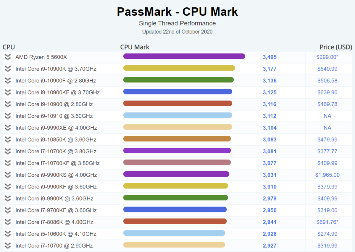
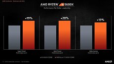
AMD Ryzen 5 5600X Takes the Crown of the Fastest CPU in Passmark Single-Thread Results

AMD has been improving its Zen core design, and with the latest Zen 3 IP found in Ryzen 5000 series CPUs, it seems like the company struck gold. Thanks to the reporting of VideoCardz, we come to know that AMD's upcoming Ryzen 5 5600X CPU has been benchmarked and compared to other competing offerings. In the CPU benchmark called PassMark, which rates all of the CPUs by multi-threaded and single-threaded performance, AMD's Ryzen 5 5600X CPU has taken the crown of the fastest CPU in the single-threaded results chart. Scoring an amazing 3495 points, it is now the fastest CPU for 1T workloads. That puts the CPU above Intel's current best—Core i9-10900K—which scores 3177 points. This puts the Zen 3 core about 10% ahead of the competition.

As a reminder, the AMD Ryzen 5 5600X CPU is a six-core, twelve threaded design that has a base clock of 3.7 GHz and boosts the frequency of the cores to 4.6 GHz, all within the TDP of 65 Watts. The CPU has 32 MB of level-3 (L3) cache and 3 MB of L2 cache.

Dialog Semiconductor Licenses its Non-Volatile ReRAM Technology to GLOBALFOUNDRIES for 22FDX Platform

DIALOG SEMICONDUCTOR, a leading provider of battery and power management, Wi-Fi and Bluetooth low energy (BLE) and Industrial edge computing solutions and GLOBALFOUNDRIES (GF ), the world's leading specialty foundry, today announced that they have entered into an agreement in which Dialog licenses its Conductive Bridging RAM (CBRAM) technology to GLOBALFOUNDRIES. The resistive ram (ReRAM)-based technology was pioneered by Adesto Technologies which was recently acquired by Dialog Semiconductor in 2020. GLOBALFOUNDRIES will first offer Dialog's CBRAM as an embedded, non-volatile memory (NVM) option on its 22FDX platform, with the plan to extend to other platforms.

Dialog's proprietary and production proven CBRAM technology is a low power NVM solution designed to enable a range of applications from IoT and 5G connectivity to artificial intelligence (AI). Low power consumption, high read/write speeds, reduced manufacturing costs and tolerance for harsh environments make CBRAM particularly suitable for consumer, medical, and select industrial and automotive applications. Furthermore, CBRAM technology enables cost-effective embedded NVM for advanced technology nodes required for products in these markets.

Intel Introduces new Security Technologies for 3rd Generation Intel Xeon Scalable Platform, Code-named "Ice Lake"

Intel today unveiled the suite of new security features for the upcoming 3rd generation Intel Xeon Scalable platform, code-named "Ice Lake." Intel is doubling down on its Security First Pledge, bringing its pioneering and proven Intel Software Guard Extension (Intel SGX) to the full spectrum of Ice Lake platforms, along with new features that include Intel Total Memory Encryption (Intel TME), Intel Platform Firmware Resilience (Intel PFR) and new cryptographic accelerators to strengthen the platform and improve the overall confidentiality and integrity of data.

Data is a critical asset both in terms of the business value it may yield and the personal information that must be protected, so cybersecurity is a top concern. The security features in Ice Lake enable Intel's customers to develop solutions that help improve their security posture and reduce risks related to privacy and compliance, such as regulated data in financial services and healthcare.

Imagination Launches IMG B-Series: Doing More with Multi-Core, up to 6 TeraFLOPs of Compute

Imagination Technologies announces IMG B-Series, a new expanded range of GPU IP. With its advanced multi-core architecture, B-Series enables Imagination customers to reduce power while reaching higher levels of performance than any other GPU IP on the market. It delivers up to 6 TFLOPS of compute, with an up to 30% reduction in power and 25% area reduction over previous generations and up to 2.5x higher fill rate than competing IP cores.

With IMG A-Series Imagination made an exceptional leap over previous generations, resulting in an industry-leading position for performance and power characteristics. B-Series is a further evolution delivering the highest performance per mm² for GPU IP and offering new configurations for lower power and up to 35% lower bandwidth for a given performance target, making it a compelling solution for top-tier designs.

Arm Highlights its Next Two Generations of CPUs, codenamed Matterhorn and Makalu, with up to a 30% Performance Uplift

Editor's Note: This is written by Arm vice president and general manager Paul Williamson.

Over the last year, I have been inspired by the innovators who are dreaming up solutions to improve and enrich our daily lives. Tomorrow's mobile applications will be even more imaginative, immersive, and intelligent. To that point, the industry has come such a long way in making this happen. Take app stores for instance - we had the choice of roughly 500 apps when smartphones first began shipping in volume in 2007 and today there are 8.9 million apps available to choose from.

Mobile has transformed from a simple utility to the most powerful, pervasive device we engage with daily, much like Arm-based chips have progressed to more powerful but still energy-efficient SoCs. Although the chip-level innovation has already evolved significantly, more is still required as use cases become more complex, with more AI and ML workloads being processed locally on our devices.

Intel 10 nm Ice Lake-SP Server Processors Reportedly Delayed

Intel 10 nm products have seen massive delays over the years, and Intel has built many IPs on the new node, however, not many of them have seen the light of the day due to problems the company has experienced with the manufacturing of the new node. That has caused delays in product shipments in the past, meaning that the time for 10 nm is just ahead. According to the latest DigiTimes Taiwan report, we have information that Intel is going to delay its Ice Lake-SP server processors manufactured on a 10 nm node. And it is going to be a whole quarter late according to the report. Instead of launching in Q4 this year, we can expect to see new processors in Q1 of 2021. It is yet unknown whatever the launch will happen at the beginning of Q1 or its end, however, we will report on it as we hear more information.

Update: DigiTimes has also released another report regarding server shipments. It is reported that server vendors are decelerating the shipments as they are making fewer orders in Q4 to wait for the new Intel CPUs. Judging by this move, the demand for these new processors is going to be rather high and the supply chain is preparing slowly for it.

Arm Spins-out Cerfe Labs to Advance Development of CeRAM Memory Technology

Today Arm announced the spin-out of Cerfe Labs to develop and license new types of non-volatile memories based on correlated electron materials (CeRAM) and ferroelectric transistors (FeFETs). Arm CeRAM researchers will join Cerfe Labs and assume ownership of the Arm joint development project with Symetrix Corporation.

As part of the spin-out, Arm will transfer its full CeRAM IP portfolio of more than 150 patent families to Cerfe Labs that will be the foundation for a roadmap of related CeRAM technologies. Cerfe Labs initial focus will be on producing meaningful prototypes which will be licensed to partners with a goal of accelerating timing of enabling these novel non-volatile materials for systems.

New Arm Technologies Enable Safety-capable Computing Solutions for an Autonomous Future

Today, Arm unveiled new computing solutions to accelerate autonomous decision-making with safety capability across automotive and industrial applications. The new suite of IP includes the Arm Cortex -A78AE CPU, Arm Mali -G78AE GPU, and Arm Mali-C71AE ISP, engineered to work together in combination with supporting software, tools and system IP to enable silicon providers and OEMs to design for autonomous workloads. These products will be deployed in a range of applications, from enabling more intelligence and configurability in smart manufacturing to enhancing ADAS and digital cockpit applications in automotive.

"Autonomy has the potential to improve every aspect of our lives, but only if built on a safe and secure computing foundation," said Chet Babla, vice president, Automotive and IoT Line of Business at Arm. "As autonomous decision-making becomes more pervasive, Arm has designed a unique suite of technology that prioritizes safety while delivering highly scalable, power efficient compute to enable autonomous decision-making across new automotive and industrial opportunities."

Arm Announces Next-Generation Neoverse V1 and N2 Cores

Ten years ago, Arm set its sights on deploying its compute-efficient technology in the data center with a vision towards a changing landscape that would require a new approach to infrastructure compute.

That decade-long effort to lay the groundwork for a more efficient infrastructure was realized when we announced Arm Neoverse, a new compute platform that would deliver 30% year-over-year performance improvements through 2021. The unveiling of our first two platforms, Neoverse N1 and E1, was significant and important. Not only because Neoverse N1 shattered our performance target by nearly 2x to deliver 60% more performance when compared to Arm's Cortex-A72 CPU, but because we were beginning to see real demand for more choice and flexibility in this rapidly evolving space.

Microsoft Announces Acquisition of Bethesda Parent Company ZeniMax Media

Microsoft today dropped a giant bomb on the balance of game development: the company announced the acquisition of ZeniMax Media, parent company of Bethesda Softworks, and all its related IP. The purchase, which is expected to close for a tidy $7.5 billion, will carry over all ZeniMax Media subsidiaries. This includes Bethesda (The Elder Scrolls, Fallout), id Software (DOOM), Arkane Studios (Prey, Dishonored, upcoming Deathloop), MachineGames (Wolfenstein), among others.

The deal is the costliest acquisition for Microsoft (to date) in its push to increase the number of in-house development studios (up to 23 from 15 prior to this deal). Microsoft has announced that as part of the deal, games published by ZeniMax Media and subsidiaries (and in the future, by Microsoft) will be available on its Xbox Games Pass subscription service for Xbox and PC gaming. Microsoft is acquiring some of the most iconic gaming franchises ever with this deal, including all in-development IP. It's a huge boon for the company; it remains to be seen exactly how will this evolve over the years. But one thing is for certain: Microsoft isn't slowing down on its doubling down on game development.

NVIDIA to Acquire Arm for $40 Billion, Creating World's Premier Computing Company for the Age of AI

NVIDIA and SoftBank Group Corp. (SBG) today announced a definitive agreement under which NVIDIA will acquire Arm Limited from SBG and the SoftBank Vision Fund (together, "SoftBank") in a transaction valued at $40 billion. The transaction is expected to be immediately accretive to NVIDIA's non-GAAP gross margin and non-GAAP earnings per share.

The combination brings together NVIDIA's leading AI computing platform with Arm's vast ecosystem to create the premier computing company for the age of artificial intelligence, accelerating innovation while expanding into large, high-growth markets. SoftBank will remain committed to Arm's long-term success through its ownership stake in NVIDIA, expected to be under 10 percent.

Rambus Advances HBM2E Performance to 4.0 Gbps for AI/ML Training Applications

Rambus Inc. (NASDAQ: RMBS), a premier silicon IP and chip provider making data faster and safer, today announced it has achieved a record 4 Gbps performance with the Rambus HBM2E memory interface solution consisting of a fully-integrated PHY and controller. Paired with the industry's fastest HBM2E DRAM from SK hynix operating at 3.6 Gbps, the solution can deliver 460 GB/s of bandwidth from a single HBM2E device. This performance meets the terabyte-scale bandwidth needs of accelerators targeting the most demanding AI/ML training and high-performance computing (HPC) applications.

"With this achievement by Rambus, designers of AI and HPC systems can now implement systems using the world's fastest HBM2E DRAM running at 3.6 Gbps from SK hynix," said Uksong Kang, vice president of product planning at SK hynix. "In July, we announced full-scale mass-production of HBM2E for state-of-the-art computing applications demanding the highest bandwidth available."

Western Digital Sets a New Standard in Data Protection with Ground-Breaking ArmorLock Security Platform

Underscoring its mission to enable the world to solve its biggest data challenges by building a data infrastructure with next-gen security, Western Digital (NASDAQ: WDC) today introduced the ArmorLock Security Platform. A data encryption platform that rethinks how data security should be done, the ArmorLock Security Platform was created to help with the diverse security demands of data-centric and content-critical storage use cases in industries as varied as finance, government, healthcare, IT enterprise, legal, and media and entertainment. As data security concerns continue to rise in visibility, Western Digital plans to apply the platform across a range of storage solutions.

The first product to leverage this advanced technology, the new G-Technology ArmorLock encrypted NVMe SSD, is designed to deliver an easy-to-use, high-performance, high-grade security storage solution for creators in the media and entertainment industry. Facing the threat of hijacked media files and leaked films, studios, agencies, and especially investors are demanding a better way to protect critical content. While much of the industry's focus has been on cloud security, data often remains vulnerable on the portable storage devices holding critical commercial content.

Arm and DARPA Sign Partnership Agreement to Accelerate Technological Innovation

Arm today announced a three-year partnership agreement with the U.S. Defense Advanced Research Projects Agency (DARPA), establishing an access framework to all commercially available Arm technology. With DARPA's Electronics Resurgence Initiative gaining momentum, the new agreement will enable the research community that supports DARPA's programs to quickly and easily take advantage of Arm's leading IP, tools and support, accelerating innovation in a variety of fields.

"The span of DARPA research activity opens up a huge range of opportunities for future technological innovation," said Rene Haas, president, IP Products Group, Arm. "Our expanded DARPA partnership will provide them with access to the broadest range of Arm technology to develop compute solutions supported by the world's largest ecosystem of tools, services and software."

Samsung Aims to Become Number One Android AP Vendor by Joining Forces with AMD and Arm

Samsung Electronics has reportedly laid out a plan to become the number one Android application processor (AP) vendor in the industry with its plan to join forces with AMD and Arm. The report of Business Korea indicates that Samsung wants to use both company's knowledge and IP to produce the best possible silicon. In early November of last year, Samsung has decided to shut down its division responsible for making custom CPU designs, and to start licensing IP from Arm. Also last year, Samsung has announced a strategic partnership with AMD to use its RDNA graphics processors in smartphones.

So Samsung plans to license IPs from both companies and just put them in SoC that will be up to the task to deliver the best performance, as the company predicts. The CPU is reportedly going to be based on Arm's Cortex-X custom design that should deliver high-performance Samsung wants. In the past, the company had some problems with the heat-management of its CPUs as they were designed a bit inefficiently. To cover everything, Samsung also plans to increase the number of employees working on a neural processing unit (NPU) and make a good performing NPUs as well, to combine with the rest of IPs.

Intel Rocket Lake CPUs Will Bring up to 10% IPC Improvement and 5 GHz Clocks

Intel is struggling with its node development and it looks like next-generation consumer systems are going to be stuck on 14 nm for a bit more. Preparing for that, Intel will finally break free from Skylake-based architectures and launch something new. The replacement for the current Comet Lake generation is set to be called Rocket Lake and today we have obtained some more information about it. Thanks to popular hardware leaker rogame (_rogame), we know a few stuff about Rocket Lake. Starting off, it is known that Rocket Lake features the backport of 10 nm Willow Cove core, called Cypress Cove. That Cypress Cove is supposed to bring only 10% IPC improvements, according to the latest rumors.

With 10% IPC improvement the company will at least offer some more competitive product than it currently does, however, that should be much slower than 10 nm Tiger Lake processors which feature the original Willow Cove design. It shows that backporting of the design doesn't just bring loses of the node benefits like smaller design and less heat, but rather means that only a fraction of the performance can be extracted. Another point that rogame made is that Rocket Lake will run up to 5 GHz in boost, and it will run hot, which is expected.

JEDEC Publishes New DDR5 Standard for Advancing Next-Generation High Performance Computing Systems

JEDEC Solid State Technology Association, the global leader in the development of standards for the microelectronics industry, today announced the publication of the widely-anticipated JESD79-5 DDR5 SDRAM standard. The standard addresses demand requirements being driven by intensive cloud and enterprise data center applications, providing developers with twice the performance and much improved power efficiency. JESD79-5 DDR5 is now available for download from the JEDEC website.

DDR5 was designed to meet increasing needs for efficient performance in a wide range of applications including client systems and high-performance servers. DDR5 incorporates memory technology that leverages and extends industry know-how and experience developing previous DDR memories. The standard is architected to enable scaling memory performance without degrading channel efficiency at higher speeds, which has been achieved by doubling the burst-length to BL16 and bank-count to 32 from 16. This revolutionary architecture provides better channel efficiency and higher application level performance that will enable the continued evolution of next-generation computing systems. In addition, the DDR5 DIMM has two 40-bit fully independent sub-channels on the same module for efficiency and improved reliability.

New features, such as DFE (Decision Feedback Equalization), enable IO speed scalability for higher bandwidth and improved performance. DDR5 supports double the bandwidth as compared to its predecessor, DDR4, and is expected to be launched at 4.8 Gbps (50% higher than DDR4's end of life speed of 3.2 Gbps).

xMEMS Launches Montara, World's First Monolithic True MEMS Speaker

Today xMEMS Labs emerged from stealth mode to reinvent sound with the introduction of Montara, the world's first monolithic true MEMS speaker, delivering high fidelity, full-bandwidth sound and low total harmonic distortion (THD) for sealed in-ear personal audio devices, including true wireless stereo (TWS) earbuds. Montara is also the world's first IP-57 rated microspeaker, enabling water and dust-resistant earbuds. Consumers will benefit from enhanced audio fidelity with raised levels of clarity and detail for instruments and vocals, extremely low latency, waterproof earbuds, and longer listening times.

"With on-the-go media consumption on the rise such as subscription music, podcasts, video, audiobooks and mobile gaming, consumers are increasingly demanding enhanced audio quality and extended listen times between charges," said Joseph Jiang co-founder and CEO. "Until now, the industry has relied on antiquated, centuries-old multi-component voice coil speakers requiring labor-intensive, high variability factory assembly lines. Our revolutionary Montara product is a game changer for delivering a new combination of audio fidelity, size, energy consumption and uniformity not possible with traditional voice coil approaches."

Arm Announces new IP Portfolio with Cortex-A78 CPU

During this unprecedented global health crisis, we have experienced rapid societal changes in how we interact with and rely on technology to connect, aid, and support us. As a result of this we are increasingly living our lives on our smartphones, which have been essential in helping feed our families through application-based grocery or meal delivery services, as well as virtually seeing our colleagues and loved ones daily. Without question, our Arm-based smartphones are the computing hub of our lives.

However, even before this increased reliance on our smartphones, there was already growing interest among users to explore the limits of what is possible. The combination of these factors with the convergence of 5G and AI, are generating greater demand for more performance and efficiency in the palm of our hands.
Arm Cortex-A78

Arm Offers Startups Zero-cost Access to its IP Portfolio

Arm today announced the launch of Arm Flexible Access for Startups, an extension of its already highly successful Flexible Access program. This new initiative offers early-stage silicon startups zero-cost access to a huge range of Arm's leading IP, along with global support and training resources, enabling them to start on their journey to commercial silicon and business scale.

"In today's challenging business landscape, enabling innovation is critical - now more than ever, startups with brilliant ideas need the fastest, most trusted route to success and scale," said Dipti Vachani, senior vice president and general manager, Automotive and IoT Line of Business, Arm. "Arm Flexible Access for Startups offers new silicon entrants a faster, more cost-efficient path to working prototypes, resulting in strengthened investor confidence for future funding."
Arm Chip

Source Code of CS: GO and Team Fortress 2 Leaks

Source Code of Counter-Strike: Global Offensive and Team Fortress 2 got leaked today. It seems like Valve hasn't been careful with control of its output, and a few leaks came out. All of the licensees of the Source Engine, a multi-platform game engine used in all Valve's games like Dota 2, Half-Life, and CS: GO, have been empowered by Valve with access to the source code of 2017/2018 versions of CS: GO and Team Fortress 2. Someone down the line, however, took that opportunity and access to leak the source code. The original news source is the SteamDB Twitter account, so we don't have any link to the actual source code.

This pretty big news since CS: GO can be considered as the most popular game on the Steam platform, and IP that Valve holds on it is very valuable. The 2017/2018 version that is leaked is probably outdated by a mile now, but it still represents an act of theft and should be treated as such. We are yet to see the response from Valve and how they will handle this situation.
Counter-Strike: Global Offensive source code

New Philips ActionFit Wireless Sports Earbud with UV Cleaning Technology

Envision Peripherals, Inc. (EPI), the sole distributor of Philips-branded monitors and audio products in North America, today announces an addition to the Philips audio line with the Philips ActionFit Wireless Earbud with ultraviolet (UV) cleaning technology (TAST702BK/00). The earbuds harbor a compact soak resistant design, clear sound and comfortable fit. The Philips ActionFit Wireless Earbuds are now available on Amazon, for $179.99 USD. [Editor's note: The product appears to already be on sale for $139.99 on Amazon at this time.]

"Active people today need a quality audio solution that fits their lifestyles. The new Philips TAST702s are the perfect solution to take to the gym or go on a long bike ride, because of their comfort and their hygienic features," said David Ray, Director of Marketing for EPI.

DDR5 Arrives at 4800 MT/s Speeds, First SoCs this Year

Cadence, a fabless semiconductor company focusing on the development of IP solutions and IC design and verification tools, today posted an update regarding their development efforts for the 5th generation of DDR memory which is giving us some insights into the development of a new standard. The new DDR5 standard is supposed to bring better speeds and lower voltages while being more power-efficient. In the Cadence's blog called Breakfast Bytes, one of Cadence's memory experts talked about developments of the new standards and how they are developing the IP for the upcoming SoC solutions. Even though JEDEC, a company developing memory standards, hasn't officially published DDR5 standard specifications, Cadence is working closely with them to ensure that they stay on track and be the first on the market to deliver IP for the new standard.

Marc Greenberg, a Cadence expert for memory solutions was sharing his thoughts in the blog about the DDR5 and how it is progressing. Firstly, he notes that DDR5 is going to feature 4800 MT/s speeds at first. The initial speeds will improve throughout the 12 months when the data transfer rate will increase in the same fashion we have seen with previous generation DDR standards. Mr. Greenberg also shared that the goals of DDR5 are to have larger memory dies while managing latency challenges, same speed DRAM core as DDR4 with a higher speed I/O. He also noted that the goal of the new standard is not the bandwidth, but rather capacity - there should be 24Gb of memory per die initially, while later it should go up to 32Gb. That will allow for 256 GB DIMMs, where each byte can be accessed under 100 ns, making for a very responsive system. Mr. Greenberg also added that this is the year of DDR5, as Cadence is receiving a lot of orders for their 7 nm IP which should go in production systems this year.
Cadence DDR5

AMD Reports Theft of Graphics IP, Stolen Information Not Core to Competitiveness

AMD today disclosed that in December 2019, it was contacted by a person in possession of test files related to development of future graphics products, some of which were posted online and later taken down. This person has additional files that were never posted online, but the company maintains the data breach won't affect the competitiveness or security of its upcoming graphics processors. The company said that it is working closely with law enforcement as part of a criminal investigation into the incident.

The statement by AMD follows:
At AMD, data security and the protection of our intellectual property are a priority. In December 2019, we were contacted by someone who claimed to have test files related to a subset of our current and future graphics products, some of which were recently posted online, but have since been taken down. While we are aware the perpetrator has additional files that have not been made public, we believe the stolen graphics IP is not core to the competitiveness or security of our graphics products. We are not aware of the perpetrator possessing any other AMD IP. We are working closely with law enforcement officials and other experts as a part of an ongoing criminal investigation.

Intel Rocket Lake-S Platform Detailed, Features PCIe 4.0 and Xe Graphics

Intel's upcoming Rocket Lake-S desktop platform is expected to arrive sometime later this year, however, we didn't have any concrete details on what will it bring. Thanks to the exclusive information obtained by VideoCardz'es sources at Intel, there are some more details regarding the RKL-S platform. To start, the RKL-S platform is based on a 500-series chipset. This is an iteration of the upcoming 400-series chipset, and it features many platform improvements. The 500-series chipset based motherboards will supposedly have an LGA 1200 socket, which is an improvement in pin count compared to LGA 1151 socket found on 300 series chipset.

The main improvement is the CPU core itself, which is supposedly a 14 nm adaptation of Tiger Lake-U based on Willow Cove core. This design is representing a backport of IP to an older manufacturing node, which results in bigger die space due to larger node used. When it comes to the platform improvements, it will support the long-awaited PCIe 4.0 connection already present on competing platforms from AMD. It will enable much faster SSD speeds as there are already PCIe 4.0 NVMe devices that run at 7 GB/s speeds. With RKL-S, there will be 20 PCIe 4.0 lanes present, where four would go to the NVMe SSD and 16 would go to the PCIe slots from GPUs. Another interesting feature of the RKL-S is the addition of Xe graphics found on the CPU die, meant as iGPU. Supposedly based on Gen12 graphics, it will bring support for HDMI 2.0b and DisplayPort 1.4a connectors.
Intel Rocket Lake-S Platform
Return to Keyword Browsing
May 21st, 2024 22:35 EDT change timezone

New Forum Posts

Popular Reviews

Controversial News Posts