News Posts matching #IP

Return to Keyword Browsing

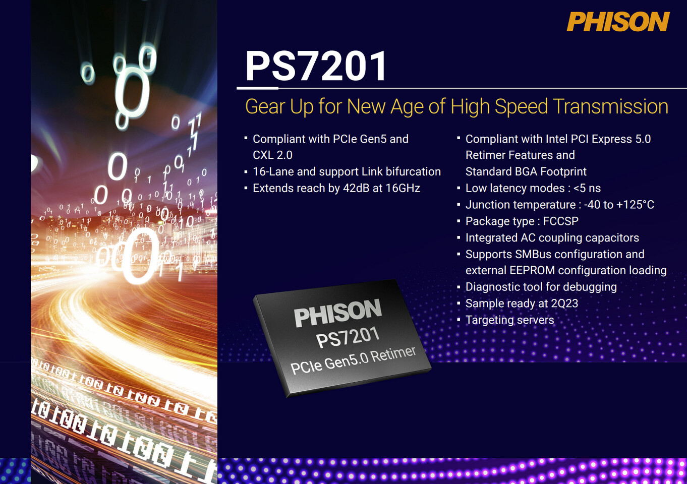
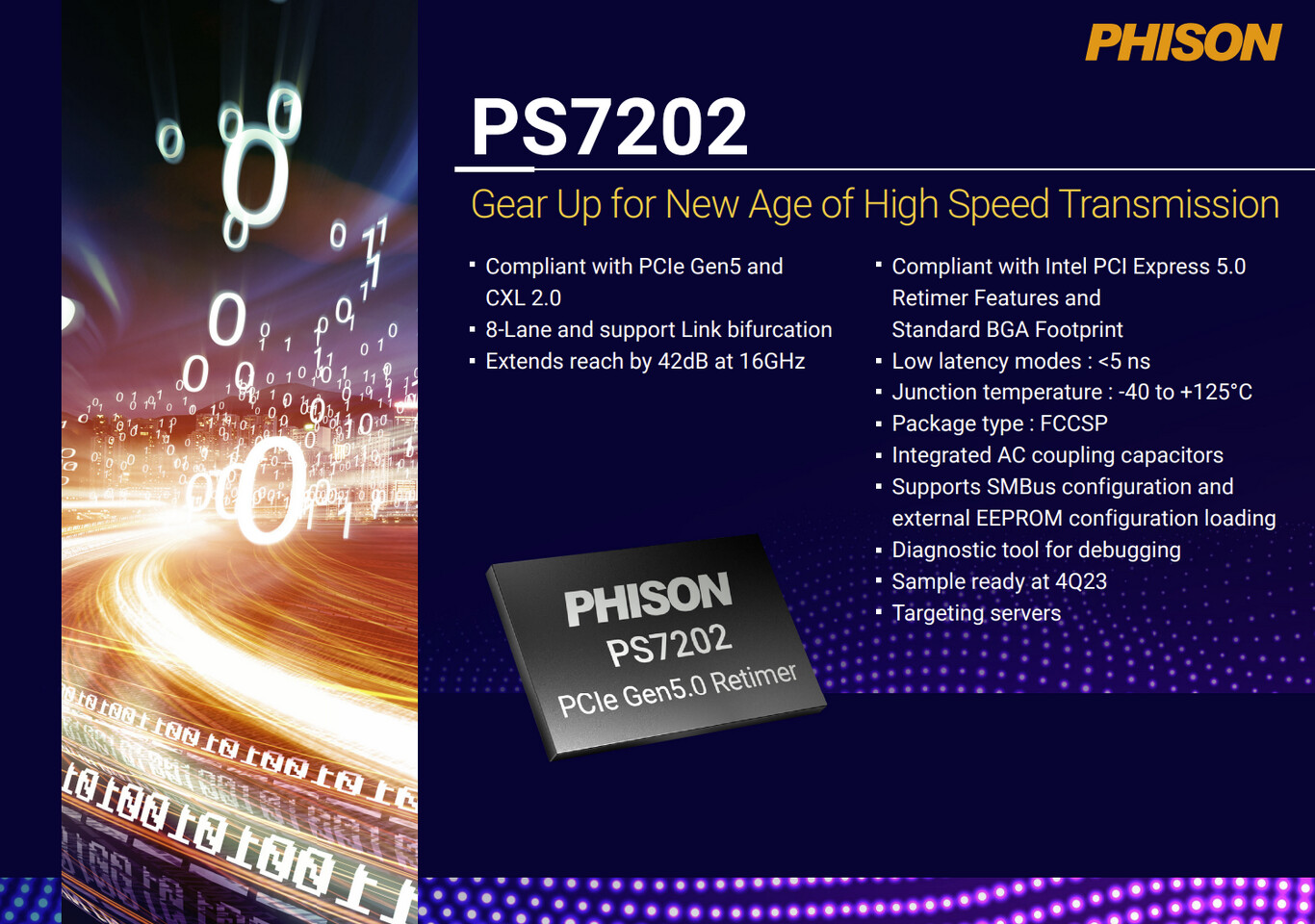
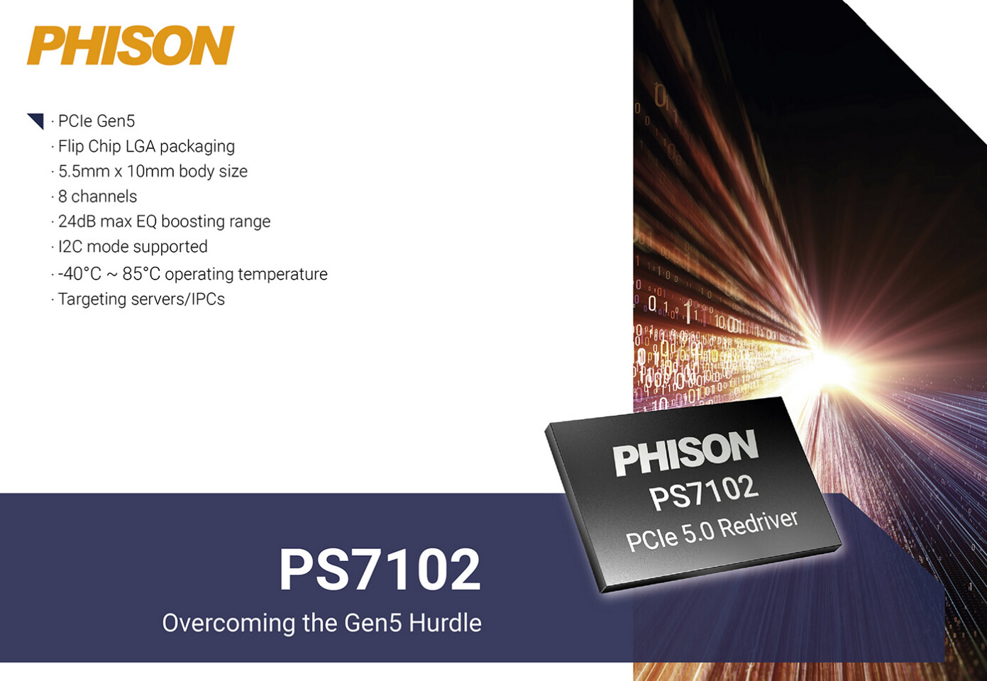
Phison Introduces New High-Speed Signal Conditioner IC Products, Expanding its PCIe 5.0 Ecosystem for AI-Era Data Centers

Phison Electronics, a global leader in NAND controllers and storage solutions, announced today that the company has expanded its portfolio of PCIe 5.0 high-speed transmission solutions with PCIe 5.0, CXL 2.0 compatible redriver and retimer data signal conditioning IC products. Leveraging the company's deep expertise in PCIe engineering, Phison is the only signal conditioners provider that offers the widest portfolio of multi-channel PCIe 5.0 redriver and retimer solutions and PCIe 5.0 storage solutions designed specifically to meet the data infrastructure demands of artificial intelligence and machine learning (AI+ML), edge computing, high-performance computing, and other data-intensive, next-gen applications. At the 2023 Open Compute Project Global Summit, the Phison team is showcasing its expansive PCIe 5.0 portfolio, demonstrating the redriver and retimer technologies alongside other enterprise NAND flash, illustrating a holistic vision for a PCIe 5.0 data ecosystem to address the most demanding applications of the AI-everywhere era.

"Phison has focused industry-leading R&D efforts on developing in-house, chip-to-chip communication technologies since the introduction of the PCIe 3.0 protocol, with PCIe 4.0 and PCIe 5.0 solutions now in mass production, and PCIe 6.0 solutions now in the design phase," said Michael Wu, President & General Manager, Phison US. "Phison's accumulated experience in high-speed signaling enables our team to deliver retimer and redriver design solutions that are optimized for top signal integration, low power usage, and high temperature endurance, to deliver interface speeds for the most challenging compute environments."

Tenstorrent Selects Samsung Foundry to Manufacture Next-Generation AI Chiplet

Tenstorrent, a company that sells AI processors and licenses AI and RISC-V IP, announced today that it selected Samsung Foundry to bring Tenstorrent's next generation of AI chiplets to market. Tenstorrent builds powerful RISC-V CPU and AI acceleration chiplets, aiming to push the boundaries of compute in multiple industries such as data center, automotive and robotics. These chiplets are designed to deliver scalable power from milliwatts to megawatts, catering to a wide range of applications from edge devices to data centers.

To ensure the highest quality and cutting-edge manufacturing capabilities for its chiplet, Tenstorrent has selected Samsung's Foundry Design Service team, known for their expertise in silicon manufacturing. The chiplets will be manufactured using Samsung's state-of-the-art SF4X process, which boasts an impressive 4 nm architecture.

Synopsys and TSMC Streamline Multi-Die System Complexity with Unified Exploration-to-Signoff Platform and Proven UCIe IP on TSMC N3E Process

Synopsys, Inc. today announced it is extending its collaboration with TSMC to advance multi-die system designs with a comprehensive solution supporting the latest 3Dblox 2.0 standard and TSMC's 3DFabric technologies. The Synopsys Multi-Die System solution includes 3DIC Compiler, a unified exploration-to-signoff platform that delivers the highest levels of design efficiency for capacity and performance. In addition, Synopsys has achieved first-pass silicon success of its Universal Chiplet Interconnect Express (UCIe) IP on TSMC's leading N3E process for seamless die-to-die connectivity.

"TSMC has been working closely with Synopsys to deliver differentiated solutions that address designers' most complex challenges from early architecture to manufacturing," said Dan Kochpatcharin, head of the Design Infrastructure Management Division at TSMC. "Our long history of collaboration with Synopsys benefits our mutual customers with optimized solutions for performance and power efficiency to help them address multi-die system design requirements for high-performance computing, data center, and automotive applications."

Phanteks Puts Out First Response to Patent Infringement Lawsuit by Lian Li

Phanteks put out its first statement in response to reports about Lian Li filing a patent infringement lawsuit against it. Lian Li alleges that Phanteks D30 RGB line of compound fans for radiators infringe upon a design patent held by the company, and that Lian Li Uni Fan series implement the original design defined in the patent. In particular, the controversy is around the design of the mechanism that lets you daisy-chain individual fans without cables. In its defense, Phanteks says that during the development of the D30 RGB series, its lawyers were duly consulted to look for IP conflicts. The company stated that it will face the legal challenge and is confident to prove that its product is not in infringement of Lian Li IP. The statement by Phanteks follows.
We at Phanteks can confirm the filing of the patent infringement suit filed by a fellow PC enthusiast brand. We want to inform the community that our legal team is and has always properly handled any legal issue or communication that has arose.

From the start of the Phanteks D30 fan development, we set out to design an original product that innovates to provide new solutions to PC enthusiasts. We have consulted with patent lawyers during the development and prior to the announcement of the D30 fans and the fans were not found to infringe on the claims in the patent. Phanteks D30 fans are an original idea and have been issued patents in multiple countries to date.

We value and respect valid and enforceable IP rights and are confident that the result of this legal matter will confirm there is no infringement. We will continue our mission to serve the PC community by creating unique and innovative solutions.

New MIPS CEO Sameer Wasson to Drive Company's RISC-V Market Penetration and Innovation

MIPS, a leading developer of high- performance RISC-V compute IP, has announced embedded systems industry veteran Sameer Wasson as the company's new CEO. Before joining MIPS, Wasson spent 18 years at Texas Instruments (TI), most recently as Vice President, Business Unit (BU) Manager, Processors, where he was responsible for the company's Processor businesses. In that role, Wasson re-established TI as a mainstream microprocessor (MPU) and microcontroller (MCU) supplier for high growth automotive and industrial markets, and established the company's footprint in embedded AI, software defined vehicles, and electrification.

As the new CEO of MIPS, Wasson will further accelerate the company's leadership in the High-Performance RISC-V market as it continues to expand its footprint in Automotive and Enterprise markets.

IT Leaders Optimistic about Ways AI will Transform their Business and are Ramping up Investments

Today, AMD released the findings from a new survey of global IT leaders which found that 3 in 4 IT leaders are optimistic about the potential benefits of AI—from increased employee efficiency to automated cybersecurity solutions—and more than 2 in 3 are increasing investments in AI technologies. However, while AI presents clear opportunities for organizations to become more productive, efficient, and secure, IT leaders expressed uncertainty on their AI adoption timeliness due to their lack of implementation roadmaps and the overall readiness of their existing hardware and technology stack.

AMD commissioned the survey of 2,500 IT leaders across the United States, United Kingdom, Germany, France, and Japan to understand how AI technologies are re-shaping the workplace, how IT leaders are planning their AI technology and related Client hardware roadmaps, and what their biggest challenges are for adoption. Despite some hesitations around security and a perception that training the workforce would be burdensome, it became clear that organizations that have already implemented AI solutions are seeing a positive impact and organizations that delay risk being left behind. Of the organizations prioritizing AI deployments, 90% report already seeing increased workplace efficiency.

Tachyum Achieves 192-Core Chip After Switch to New EDA Tools

Tachyum today announced that new EDA tools, utilized during the physical design phase of the Prodigy Universal Processor, have allowed the company to achieve significantly better results with chip specifications than previously anticipated, after the successful change in physical design tools - including an increase in the number of Prodigy cores to 192.

After RTL design coding, Tachyum began work on completing the physical design (the actual placement of transistors and wires) for Prodigy. After the Prodigy design team had to replace IPs, it also had to replace RTL simulation and physical design tools. Armed with a new set of EDA tools, Tachyum was able to optimize settings and options that increased the number of cores by 50 percent, and SERDES from 64 to 96 on each chip. Die size grew minimally, from 500mm2 to 600mm2 to accommodate improved physical capabilities. While Tachyum could add more of its very efficient cores and still fit into the 858mm2 reticle limit, these cores would be memory bandwidth limited, even with 16 DDR5 controllers running in excess of 7200MT/s. Tachyum cores have much higher performance than any other processor cores.

Intel and Synopsys Expand Partnership to Enable Leading IP on Intel Advanced Process Nodes

Intel and Synopsys announced that they have entered into a definitive agreement to expand the companies' long-standing IP (intellectual property) and EDA (electronic design automation) strategic partnership with the development of a portfolio of IP on Intel 3 and Intel 18A for Intel's foundry customers. The availability of key IP on Intel advanced process nodes will create a more robust offering for new and existing Intel Foundry Services (IFS) customers.

"Marking another important step in our IDM 2.0 strategy, this transaction will foster a vibrant foundry ecosystem by allowing designers to fully realize the advantages of Intel 3 and Intel 18A process technologies and quickly bring differentiated products to market," said Stuart Pann, senior vice president and general manager of IFS. "Synopsys brings a strong track record of delivering high-quality IP to a broad customer base, and this agreement will help accelerate the availability of IP on advanced IFS nodes for mutual customers."

Cadence to Acquire Rambus PHY IP Assets

Cadence Design Systems, Inc. and Rambus Inc., a premier chip and silicon IP provider making data faster and safer, today announced that they have entered into a definitive agreement for Cadence to acquire the Rambus SerDes and memory interface PHY IP business. Rambus will retain its digital IP business, including memory and interface controllers and security IP. The expected technology asset purchase also brings Cadence proven and experienced PHY engineering teams in the United States, India and Canada, further expanding Cadence's domain-rich talent base.

"Memory and SerDes IP design and integration continues to be integral to the design of AI, data center and hyperscale applications, CPU architectures and networking devices, and the addition of the Rambus IP and seasoned team further accelerates Cadence's Intelligent System Design strategy, which drives design excellence," said Boyd Phelps, senior vice president and general manager of the IP Group at Cadence. "The acquisition of the Rambus PHY IP broadens Cadence's well-established enterprise IP portfolio and expands its reach across geographies and vertical markets, such as the aerospace and defense market, providing complete subsystem solutions that meet the demands of our worldwide customers."

Intel Expects to Beat TSMC at 2nm, Intel Foundry to Operate Almost as a Separate Business

Intel's integrated device manufacturing (IDM) has been experiencing a lot of trouble in recent years, and the company is not a leading-edge semiconductor manufacturer, with TSMC taking the pole position. However, the new restructuring hopes to change some of the business operations to increase its efficiency and establish Intel as the go-to foundry for customers. David Zinsner, Executive Vice President and the Chief Financial Officer, alongside Jason Grebe, Corporate Vice President & GM of the Corporate Planning Group at Intel, joined investors to explain how IDM will transform into a next-generation business. Intel IDM, including Intel Foundry Services (IFS), will get a new operation model, which will put IDM as an almost separate business unit with its own profit and loss (P&L) statement published in the quarterly/yearly financial report.

According to Intel, the company's IDM 1.0 strategy has been serving it well, but IDM 2.0 is needed to build next-generation nodes as the capital required for them is massive. Intel hopes to regain node leadership with the Intel 18A node in 2025. The company's strategy is still to have IFS as the second biggest external foundry business, presumably just behind TSMC. Putting IDM into its own P&L will result in $8-10 billion in "cost reduction opportunities, " including ramp rates, test time, and sort times based on the market pricing, not Intel's pricing. At the start, IDM is expected o start with a negative operating margin. Intel also states that keeping IFS as a business unit allows the company to simultaneously develop products on it and de-risk it for customers who want to build on IFS. The company is developing five different products (assuming packaging) on Intel 18A, all of which will be available for customers to use as well.

ITRI Set to Strengthen Taiwan-UK Collaboration on Semiconductors

The newly established Department for Science, Innovation and Technology (DSIT) in the UK has recently released the UK's National Semiconductor Strategy. Dr. Shih-Chieh Chang, General Director of Electronic and Optoelectronic System Research Laboratories at the Industrial Technology Research Institute (ITRI) of Taiwan had an initial exchange with DSIT. During the exchange, Dr. Chang suggested that Taiwan can become a trustable partner for the UK and that the partnership can leverage collective strengths to create mutually beneficial developments. According to the Strategy, the British government plans to invest 1 billion pounds over the next decade to support the semiconductor industry. This funding will improve access to infrastructure, power more research and development and facilitate greater international cooperation.

Dr. Chang stressed that ITRI looks forward to more collaboration with the UK on semiconductors to enhance the resilience of the supply chain. While the UK possesses cutting-edge capabilities in semiconductor IP design and compound semiconductor technology, ITRI has extensive expertise in semiconductor technology R&D and trial production. As a result, ITRI is well-positioned to offer consultation services for advanced packaging pilot lines, facilitate pre-production evaluation, and link British semiconductor IP design companies with Taiwan's semiconductor industry chain. "The expansion of British manufacturers' service capacity in Taiwan would create a mutually beneficial outcome for both Taiwan and the UK," said Dr. Chang.

Realtek Takes MediaTek to Court Over Third Party Patent Dispute

A legal dispute between Realtek and MediaTek has kicked off over Realtek claiming that MediaTek has gotten a third party company to sue Realtek over some unspecified patents involving technology used in smart TVs and set-top boxes. The third party involved goes under the name of IPValue Management Inc and appears to be what is generally known as a patent troll, i.e. a company that buys up patents and uses them to take legal actions against other companies, without actually producing anything related to the patents in question. Realtek claims that MediaTek is conspiring with IPValue to drive Realtek out of the market, leaving Mediatek in a close to monopoly situation in the market.

According to Reuters, Realtek told the publication that it filed the lawsuit against MediaTek to "protect free and fair competition in the industry" and "prevent further harm to the public." Neither MediaTek or IPValue have commented on the lawsuit to the publication. What makes this entire mess even more peculiar, is that MediaTek is said to have a licensing agreement in place with a subsidiary of IPValue called Future Link System LLC, which was signed in 2019. This agreement was brought up by the U.S. International Trade Commission (ITC) in a separate lawsuit last year, with the ITC calling it alarming and the court calling it improper. After the ITC criticism last year, Future Link apparently settled with several other companies such as Amlogic, but not with Realtek, which is why the company is now taking things to court. Realtek claims that MediaTek is trying to force any allegedly infringing chips out of the market and trying to make Realtek look like an unreliable partner and supplier to its customers. As such, Realtek wants the court to end the alleged conspiracy and is also asking for damages. Time will tell if Realtek is successful or not, but it seems strange that a patent troll would agree to licence its patents to some parties, but not all, since the only reason for a patent troll to exist is to make money from its patents.

Intel Falcon Shores is Initially a GPU, Gaudi Accelerators to Disappear

During the ISC High Performance 2023 international conference, Intel announced interesting roadmap updates to its high-performance computing (HPC) and artificial intelligence (AI). With the scrapping of Rialto Bridge and Lancaster Sound, Intel merged these accelerator lines into Falcon Shores processor for HPC and AI, initially claiming to be a CPU+GPU solution on a single package. However, during the ISC 2023 talk, the company forced a change of plans, and now, Falcon Shores is GPU only solution destined for a 2025 launch. Originally, Intel wanted to combine x86-64 cores with Xe GPU to form an "XPU" module that powers HPC and AI workloads. However, Intel did not see a point in forcing customers to choose between specific CPU-to-GPU core ratios that would need to be in an XPU accelerator. Instead, a regular GPU solution paired with a separate CPU is the choice of Intel for now. In the future, as workloads get more defined, XPU solutions are still a possibility, just delayed from what was originally intended.

Regarding Intel's Gaudi accelerators, the story is about to end. The company originally paid two billion US Dollars for Habana Labs and its Gaudi hardware. However, Intel now plans to stop the Gaudi development as a standalone accelerator and instead use the IP to integrate it into its Falcon Shores GPU. Using modular, tile-based architecture, the Falcon Shores GPU features standard ethernet switching, up to 288 GB of HBM3 running at 9.8 TB/s throughput, I/O optimized for scaling, and support for FP8 and FP16 floating point precision needed for AI and other workloads. As noted, the creation of XPU was premature, and now, the initial Falcon Shores GPU will become an accelerator for HPC, AI, and a mix of both, depending on a specific application. You can see the roadmap below for more information.

Imagination Technologies Launches the IMG CXM GPU

Imagination Technologies is bringing seamless visual experiences to cost-sensitive consumer devices with the new IMG CXM GPU range which includes the smallest GPU to support HDR user interfaces natively.

Consumers are looking for visuals on their smart home platforms that are as detailed, smooth, and responsive as the experience they are accustomed to on mobile devices. At the same time, ambitious content providers are aligning the look and feel of their applications' user interfaces with their cinematic content, by integrating advanced features such as 4K and HDR.

Ampere Computing Unveils New AmpereOne Processor Family with 192 Custom Cores

Ampere Computing today announced a new AmpereOne Family of processors with up to 192 single threaded Ampere cores - the highest core count in the industry. This is the first product from Ampere based on the company's new custom core, built from the ground up and leveraging the company's internal IP. CEO Renée James, who founded Ampere Computing to offer a modern alternative to the industry with processors designed specifically for both efficiency and performance in the Cloud, said there was a fundamental shift happening that required a new approach.

"Every few decades of compute there has emerged a driving application or use of performance that sets a new bar of what is required of performance," James said. "The current driving uses are AI and connected everything combined with our continued use and desire for streaming media. We cannot continue to use power as a proxy for performance in the data center. At Ampere, we design our products to maximize performance at a sustainable power, so we can continue to drive the future of the industry."

India Homegrown HPC Processor Arrives to Power Nation's Exascale Supercomputer

With more countries creating initiatives to develop homegrown processors capable of powering powerful supercomputing facilities, India has just presented its development milestone with Aum HPC. Thanks to information from the report by The Next Platform, we learn that India has developed a processor for powering its exascale high-performance computing (HPC) system. Called Aum HPC, the CPU was developed by the National Supercomputing Mission of the Indian government, which funded the Indian Institute of Science, the Department of Science and Technology, the Ministry of Electronics and Information Technology, and C-DAC to design and manufacture the Aum HPC processors and create strong, strong technology independence.

The Aum HPC is based on Armv8.4 CPU ISA and represents a chiplet processor. Each compute chiplet features 48 Arm Zeus Cores based on Neoverse V1 IP, so with two chiplets, the processor has 96 cores in total. Each core gets 1 MB of level two cache and 1 MB of system cache, for 96 MB L2 cache and 96 MB system cache in total. For memory, the processor uses 16-channel 32-bit DDR5-5200 with a bandwidth of 332.8 GB/s. To expand on that, HBM memory is present, and there is 64 GB of HBM3 with four controllers capable of achieving a bandwidth of 2.87 TB/s. As far as connectivity, the Aum HPC processor has 64 PCIe Gen 5 Lanes with CXL enabled. It is manufactured on a 5 nm node from TSMC. With a 3.0 GHz typical and 3.5+ GHz turbo frequency, the Aum HPC processor is rated for a TDP of 300 Watts. It is capable of producing 4.6+ TeraFLOPS per socket. Below are illustrations and tables comparing Aum HPC to Fujitsy A64FX, another Arm HPC-focused design.

Bosch Plans to Acquire U.S. Chipmaker TSI Semiconductors

Bosch is expanding its semiconductor business with silicon carbide chips. The technology company plans to acquire assets of the U.S. chipmaker TSI Semiconductors, based in Roseville, California. With a workforce of 250, the company is a foundry for application-specific integrated circuits, or ASICs. Currently, it mainly develops and produces large volumes of chips on 200-millimeter silicon wafers for applications in the mobility, telecommunications, energy, and life sciences industries. Over the next years, Bosch intends to invest more than 1.5 billion USD in the Roseville site and convert the TSI Semiconductors manufacturing facilities to state-of-the-art processes. Starting in 2026, the first chips will be produced on 200-millimeter wafers based on the innovative material silicon carbide (SiC).

In this way, Bosch is systematically reinforcing its semiconductor business, and will have significantly extended its global portfolio of SiC chips by the end of 2030. Above all, the global boom and ramp-up of electromobility are resulting in huge demand for such special semiconductors. The full scope of the planned investment will be heavily dependent on federal funding opportunities available via the CHIPS and Science Act as well as economic development opportunities within the State of California. Bosch and TSI Semiconductors have reached an agreement to not to disclose any financial details of the transaction, which is subject to regulatory approval.

Sega Purchases Angry Birds Game Developer for $776 Million

Today Japan's Sega Sammy Holdings Incorporated declared its intention to fully acquire Finnish development studio Rovio Entertainment Oyj in a buyout valued at a cool $776 million. The Helsinki-based developer, responsible for creating the Angry Birds video game franchise, has agreed to Sega Sammy's terms - and Rovio share values have climbed as a result of this announcement. The deal is expected to be finalized in the late summer or early autumn of this year, and signals an ambition on Sega's part to gain prominence in the mobile gaming world. Rovio had previously turned down a proposed takeover by Playtika - an Israeli company specializing in digital entertainment - for $735 million, late last month.

Angry Birds was the first mobile game to be downloaded one billion times, according to figures released by Rovio, so Sega has acquired a solid intellectual property that has also expanded into the movie world (two animated features) and endless merchandising avenues (toys, clothing and other accessories). Commenting on the buyout, Haruki Satomi, President and Group CEO, Representative Director of Sega Sammy Holdings Inc. said: "Among the rapidly growing global gaming market, the mobile gaming market has especially high potential, and it has been Sega's long-term goal to accelerate its expansion in this field."

Chinese Loongson 3D5000 Features 32 Cores and is 4x Faster Than the Average Arm Chip

Amid the push for technology independence, Chinese companies are pushing out more products to satisfy the need for the rapidly soaring demand for domestic data processing silicon. Today, we have information that Chinese Loongson has launched a 3D5000 CPU with as many as 32 cores. Utilizing chiplet technology, the 3D5000 represents a combination of two 16-core 3C5000 processors based on LA464 cores, based on LoongArch ISA that follows the combination of RISC and MIPS ISA design principles. The new chip features 64 MB of L3 cache, supports eight-channel DDR4-3200 ECC memory achieving 50 GB/s, and has five HyperTransport (HT) 3.0 interfaces. The TDP configuration of the chip is officially 300 Watts; however, normal operation is usually at around 150 Watts, with LA464 cores running at 2 GHz.

Scaling of the new chip goes beyond the chiplet, and pours over into system, as 3D5000 supports 2P and 4P configurations, where a single motherboard can become a system of up to 128 cores. To connect them, Loongson uses a 7A2000 bridge chip that is reportedly 400% faster than the previous solution, although we have no information about the last chip bridge. Based on the LGA-4129 package, the chip size is 75.4x58.5×6.5 mm. Regarding performance, Loongson compares it to the average Arm chip that goes into smartphones and claims that its designs are up to four times faster. In SPEC2006, performance reaches 425 points, while maintaining a single TeraFLOP at dual-precision 64-bit format. On the other hand, the processor was built for security, as the chip has a custom hardware-baked security to prevent Spectre and Meltdown, has an on-package Trusted Platform Module (TPM), and has a secret China-made security algorithm with an embedded custom security module that does encryption and decryption at 5 Gbps.

Rambus and SK hynix Extend Comprehensive License Agreement

Rambus Inc., a premier chip and silicon IP provider making data faster and safer, today announced it has extended its comprehensive patent license agreement with SK hynix, a world leader in advanced semiconductor technology, for an additional ten years. Effective July 1, 2024, the extension maintains similar financial terms and provides SK hynix with broad access to the full Rambus patent portfolio through mid 2034. Other terms and details are confidential.

"SK hynix is a longstanding partner and customer, and we are very pleased to extend our strong relationship well ahead of the agreement's expiration date," said Luc Seraphin, president and chief executive officer of Rambus. "Both Rambus and SK hynix are committed to advancing the industry with world-class products and technology, and this extension is a testament to the ongoing value of our intellectual property and our continued product collaborations together."

UP Team Collaborate with Leopard Imaging to Bring AI Vision to the Edge

Following its successful demonstration of a MIPI camera solution using the UP Squared Pro 7000 at Embedded World, AAEON have announced a MIPI Expansion Kit for the newly released third generation board. Equipped with the Intel Atom Processors x7000E Series, Intel Core i3-N305 Processor and Intel Processor N Series (formerly Alder Lake-N) and an FPC port supporting MIPI-CSI interface, the UP Squared Pro 7000 emphasizes AAEON's continued dedication to bringing the latest Intel technologies to a wider variety of platforms. One such platform is the LI-ADL-ADP-IMX415-MIPI-081H, a 4K MIPI Camera Module from leading intelligent embedded camera creator, Leopard Imaging Inc.

The company recently announced that the camera has been designed with full-function drivers to support the Intel Atom Processors x7000E Series, Intel Core i3-N305 Processor, and Intel Processor N Series (formerly Alder Lake-N), allowing users to take advantage of the peripheral Intel technologies that come with the processor platform, such as Intel UHD Graphics on a Windows 10 IoT Enterprise OS.

Arm to Change Pricing Model Ahead of IPO

Softbank, the owner of Arm Ltd., is preparing everything it can to ensure a successful initial public offering (IPO) of Arm. However, ahead of the IPO, we have more information about Arm's plans to change its licensing and pricing structures to collect more royalties and ensure higher cash flow for future investors. Currently, Arm licenses technology in the form of intellectual property (IP), usually in different flavors of Cortex-A CPU cores that go inside processors for phones and laptops. Chipmakers that use the IP have additional expenses such as Arm ISA license fee and per-chip royalty, which is based on the chip's average selling price.

However, according to Financial Times, we have a new pricing structure that changes how Arm bills its partners and customers. From now on, Arm will grant licenses to chipmakers and ask them to only ship to device makers with an agreement with Arm. Additionally, these device makers now pay per-device royalty based on the device's average selling price (ASP). This ensures that Arm's fee applies to the higher margin product, which means that ultimately Arm will collect more cash flow from its customers and partners. Currently, the old model charges around 1-2 percents per chip in each smartphone, considering the ASP of smartphone chips to be $40 for Qualcomm, $17 for MediaTek, and $6 for Unisoc. However, taking the ASP of a mobile phone at $335, as recorded in 2022, the fee would be much higher. People familiar with the matter noted that Arm will apply this pricing structure as early as 2024. Apple and Samsung are not impacted by this change, as both companies enjoy their own agreements with Arm.

Atari is Acquiring Nightdive Studios

Atari has announced that is buying Nightdive Studios for a cool $10 million - the abandonware specialists will become part of the publisher's larger ambitions to boost production of retro IPs. Nightdive's proprietary KEX engine will form the technological base for future remakes of Atari titles from the archives. As the news of this acquisition hit the web, the Nightdive Twitter posted a positive message regarding the buyout: "This is a big win for our team! As we look to continue producing high-quality, new, and remastered games that do justice to the original IP; we could think of no better long-term partner than."

Nightdive leaders Stephen Kick and Larry Kuperman stated in a joint statement: "Night Dive and Atari have a long history together and we know that Atari shares our passion for retro games and our focus on producing high-quality new and remastered games that do justice to the original IP. As we look to grow our business and expand our capabilities, we could think of no better long-term partner than Atari."

Cadence Announces The First GDDR7 Verification Solution

Cadence, a leading developer of tools for system design and verification, has announced the industry's first GDDR7 verification solution. This in-depth software solution affords IC designers the ability to simulate and verify their GDDR7 silicon designs before printing a single chip. The challenges of designing GDDR7 stem from a rather massive leap in operating speed and advanced features, with GDDR7 targeting speeds of 36,000 MT/s and utilizing more advanced signaling methods.

Biden-Harris Administration Launches First CHIPS for America Funding Opportunity

The Biden-Harris Administration through the U.S. Department of Commerce's National Institute of Standards and Technology today launched the first CHIPS for America funding opportunity for manufacturing incentives to restore U.S. leadership in semiconductor manufacturing, support good-paying jobs across the semiconductor supply chain, and advance U.S. economic and national security.

As part of the bipartisan CHIPS and Science Act, the Department of Commerce is overseeing $50 billion to revitalize the U.S. semiconductor industry, including $39 billion in semiconductor incentives. The first funding opportunity seeks applications for projects to construct, expand, or modernize commercial facilities for the production of leading-edge, current-generation, and mature-node semiconductors. This includes both front-end wafer fabrication and back-end packaging. The Department will also be releasing a funding opportunity for semiconductor materials and equipment facilities in the late spring, and one for research and development facilities in the fall.
Return to Keyword Browsing
May 21st, 2024 05:41 EDT change timezone

New Forum Posts

Popular Reviews

Controversial News Posts