News Posts matching #MCM

Return to Keyword Browsing

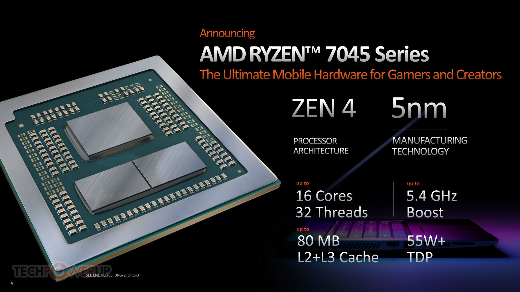
Raytheon works with AMD to develop next-gen Multi-Chip Package

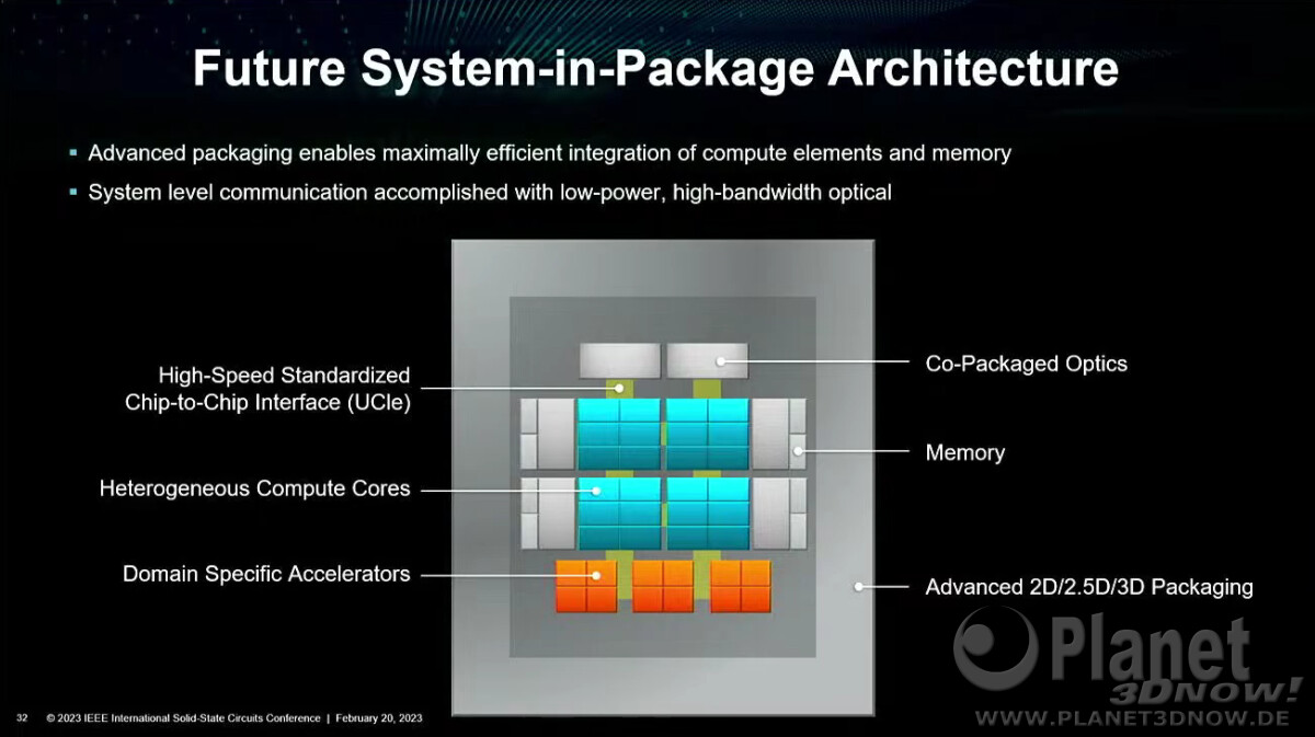
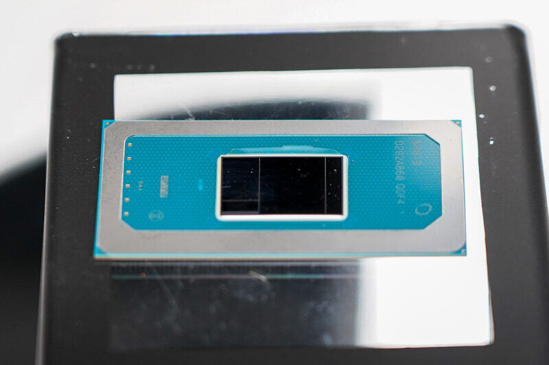
Raytheon, an RTX business, has been awarded a $20 million contract through the Strategic and Spectrum Missions Advanced Resilient Trusted Systems (S2MARTS) consortium to develop a next-generation multi-chip package for use in ground, maritime and airborne sensors. Under the contract, Raytheon will package state-of-the-art commercial devices from industry partners like AMD to create a compact microelectronics package that will convert radio frequency energy to digital information with more bandwidth and higher data rates. The integration will result in new system capabilities designed with higher performance, lower power consumption and reduced weight.

"By teaming with commercial industry, we can incorporate cutting-edge technology into Department of Defense applications on a much faster timescale," said Colin Whelan, president of Advanced Technology at Raytheon. "Together, we will deliver the first multi-chip package that features the latest in interconnect ability - which will provide new system capabilities to our warfighters."

Bitspower at 2024 CES: Griffin Radiator Fans, Summit Blocks, New Water Cooling Gear, Enigma Light Panels

Bitspower brought a large bag of new toys at the 2024 International CES. The first thing that caught our attention was a familiar-looking case with infinity reflection lighting. On a closer look, it turned out to be a Lian Li PC-O11D Evo XL that's been given a neat aesthetic uplift thanks to the new Enigma Light Panel kit by Bitspower. You arrange these along the edges of your side- and front panels, and the provide an impressive, infinity reflection effect. It works with standard 3-pin ARGB, so you can mix it with your regular lighting setup. Next up, are a slew of CR Slim series reservoirs that are designed in the distribution plate format, which they line up with one of your glass panels, providing a better view of your coolant. There are various sizes, ranging from 120 mm x 120 mm, going all the way up to 803 mm. x 140 mm, with fitting ports at strategic locations to align with your CPU and VGA blocks, and radiators. The reservoirs come with preparation for a standard D5 pump, and feature a side cover that has the ARGB LED lighting, the diodes aren't studded into the acrylic as such. Bitspower released a mounting brackets of various sizes to help you correctly mount the reservoirs and accessories in place.

Iceberg Thermal Brings New Air, Liquid, and Er..Drink Coolers to CES

Iceberg Thermal specializes in CPU cooling and fans, with elaborate tower-type, and dual-tower type air coolers, and AIO liquid CPU coolers. It brought practically the entire lineup to 2024 CES, including some interesting bits of hardware. The IceSleet G3 and G4 series are single fin-stack CPU coolers. The IceSleet G3 is at the entry-mid range, capable of thermal loads of 160 W. It uses a single aluminium fin-stack heatsink to which heat drawn from a direct-touch base is fed by three 6 mm-thick copper heat pipes. A single 120 mm fan ventilates it. The IceSleet G4 OC is a step up, and although it's recommended for the same 160 W thermal loads as the G3, it has four 6 mm-thick heatpipes, which should improve heat transfer, allowing you to lower the fan speed. It uses a single 120 mm fan that features addressable RGB lighting. The cooler comes in ice blue+white and black+ice blue 2-tone color variants.

The IceSleet G4 Silent is a further step up, with a cooling capacity of 170 W, a higher density heatsink, four 6 mm-thick copper heatpipes, and a fan tuning that's optimized for low noise. The IceSleet G4 Midnight is similar in characteristics to the G4 OC, but comes in an all-black that includes black anodized aluminium fins, heatpipes, plastic cladding, and of course the fan frame. Although tinted dark, the fan impeller is studded with addressable RGB. The company also unveiled its new IceGale Lightning ARGB series 120 mm fan, with noise levels under 28.9 dBA. These 120 mm spinners of conventional thickness turn at speeds ranging between 200 to 2,200 RPM, pushing 76.74 CFM of airflow, at 2.8 mm H₂O static pressure. The fan comes with a fluid dynamic bearing that's rated for over 70,000 hours by its designers.

AMD Readies Radeon RX 7600 XT, RX 7700, and RX 7800

Even as NVIDIA inches close to the launch of its RTX 40-series SUPER graphics cards in January, AMD could be preparing a product stack update of its own. While NVIDIA's refresh focuses on the higher end of its lineup, AMD looks to spread out more into the mainstream-performance segments. A regulatory filing with the Eurasian Economic Commission mentions the terms "RX 7600 XT," "RX 7700," and "RX 7800," which fill gaps between the RX 7600, RX 7700 XT, and RX 7800 XT.

There exists a rather big gap between the $230 Radeon RX 7600 and the $450 RX 7700 XT, which AMD is looking to fill with the RX 7600 XT and RX 7700 (non-XT). How AMD goes about carving out these two will be interesting to see. The RX 7600 already maxes out the 6 nm "Navi 33" silicon that it's based on, which means to create the RX 7600 XT, AMD might have to tap into the larger (and much more expensive) "Navi 32" MCM. There is a vast gap between the 32 CU (compute units) available to the RX 7600, and the 54 CU that the RX 7700 XT has (while the silicon itself has 60). Besides CU count, AMD has other levers, such as the MCD (memory cache die) count, which could be down to just 2 for the RX 7600 XT, or 3 for the RX 7700. The Radeon RX 7800 is a different beast. AMD faced quite some flack for positioning the RX 7700 XT within $50 of the RX 7800 XT, and now the former can be had for a street price of roughly $430. To be able to squeeze the RX 7800 between the two, AMD might need to widen the gap by pushing the RX 7700 XT down.

AMD 5th Gen EPYC "Turin" Pictured: Who Needs Accelerators When You Have 192 Cores?

AMD's upcoming server processor, the 5th Gen EPYC "Turin," has been pictured as an engineering sample is probably being evaluated by the company's data-center or cloud customers. The processor has a mammoth core-count of 192-core/384-thread in its high-density cloud-focused variant that uses "Zen 5c" CPU cores. Its regular version that uses larger "Zen 5" cores that can sustain higher clock speeds, also comes with a fairly high core-count of 128-core/256-thread, up from the 96-core/192-thread of the "Zen 4" based EPYC "Genoa."

The EPYC "Turin" server processor based on "Zen 5" comes with an updated sIOD (server I/O die), surrounded by as many as 16 CCDs (CPU complex dies). AMD is expected to build these CCDs on the TSMC N4P foundry node, which is a more advanced version of the TSMC N4 node the company currently uses for its "Phoenix" client processors, and the TSMC N5 node it uses for its "Zen 4" CCD. TSMC claims that the N4P node offers an up to 22% improvement in power efficiency over N5, as well as a 6% increase in transistor density. Each of the "Zen 5" CCDs is confirmed to have 8 CPU cores sharing 32 MB L3 cache memory. A total of 16 such CCDs add up to the processor's 128-core/256-thread number. The high-density "Turin" meant for cloud data-centers, is a whole different beast.

NVIDIA Blackwell GB100 Die Could Use MCM Packaging

NVIDIA's upcoming Blackwell GPU architecture, expected to succeed the current Ada Lovelace architecture, is gearing up to make some significant changes. While we don't have any microarchitectural leaks, rumors are circulating that Blackwell will have different packaging and die structures. One of the most intriguing aspects of the upcoming Blackwell is the mention of a Multi-Chip Module (MCM) design for the GB100 data-center GPU. This advanced packaging approach allows different GPU components to exist on separate dies, providing NVIDIA with more flexibility in chip customization. This could mean that NVIDIA can more easily tailor its chips to meet the specific needs of various consumer and enterprise applications, potentially gaining a competitive edge against rivals like AMD.

While Blackwell's release is still a few years away, these early tidbits paint a picture of an architecture that isn't just an incremental improvement but could represent a more significant shift in how NVIDIA designs its GPUs. NVIDIA's potential competitor is AMD's upcoming MI300 GPU, which utilized chiplets in its designs. Chiplets also provide ease of integration as smaller dies provide better wafer yields, meaning that it makes more sense to switch to smaller dies and utilize chiplets economically.

Intel "Granite Rapids-D" Xeon Processors Come in Core-count and Memory-channel Based Physical Variants

The "Granite Rapids-D" line of upcoming processors are designed for data-center servers on the edge. These non-socketed processors come in BGA4368 packages. The company is reportedly readying at least two key variants of these chips based on core-counts and memory channels. The "Granite Rapids-D" HCC (high core-count) is an MCM of a "Granite Rapids" LCC (low-core count) compute tile, and a single I/O tile with a 4-channel DDR5 memory interface.

The "Granite Rapids-D" XCC (extreme core-count) has one "Granite Rapids" HCC (high core-count) compute tile, and two I/O tiles that make up the chip's 8-channel DDR5 memory interface. A probable reason for the confusion between LCC, HCC, and XCC terminologies for "Granite Rapids-D" is because the compute tiles are carried over from the main "Granite Rapids-SP" server processors, where they mean different things for the core-counts of mainline servers.

AMD Readies Ryzen 5 5600X3D to Take on Intel's 13th Gen Core i5 + DDR4 Options

AMD is finally coming around to the idea of a 6-core processor with 3D Vertical Cache technology, only this time it's for the older Socket AM4 platform. The new Ryzen 5 5600X3D could be positioned competitively against the lower end of Intel's 13th Gen Core i5 processor series, so it could attract a class of DIY gaming PC builders that can take advantage of cheap Socket AM4 motherboards and DDR4 memory to build formidable mainstream gaming PC builds.

The Ryzen 5 5600X3D is based on the same "Vermeer" 3DV cache MCM as the 5800X3D. It is a 6-core/12-thread processor with a base frequency of 3.30 GHz, and 4.40 GHz boost, which are both 100 MHz less than those of the 5800X3D. The processor gets the full 96 MB of last-level cache (that's 32 MB of on-die L3 cache + 64 MB of 3DV cache), which the 5800X3D offers. It bears the OPN "100-000001176." The company didn't reveal pricing, but given that the 5800X3D can be had for as low as $290, the 5600X3D could possibly target a $200-225 price, making it an attractive option, given that you can pair it with even cheap B450 chipset motherboards priced well under $100, and 32 GB of DDR4 memory that can be had around the $60-mark. The 5600X3D could also provide an affordable upgrade path to those still on the AM4 platform, with Ryzen 3000-series processors.

AMD to Shift Some of its 4 nm CPU Silicon-fabrication to Samsung from TSMC

AMD has reportedly signed up with Samsung Electronics to shift some of its 4 nm processor silicon fabrication from TSMC. The apex Taiwan-based foundry is reportedly operating at capacity for its 4 nm-class nodes, with customers such as Apple and Qualcomm sourcing 4 nm mobile SoCs on the node, leaving AMD with limited allocation and/or bargaining power with TSMC. The company relies on 4 nm for its Ryzen 7040 series "Phoenix" mobile processors, and is in the process of adapting its design for Samsung's 4 nm-class nodes (of which there are five types for AMD to choose from).

Switching to Samsung probably gives AMD more scalability, particularly given that "Phoenix" has missed its release timeline, leaving AMD with the 5 nm + 6 nm Ryzen 7045 series "Dragon Range" MCM in the premium segments, and older 6 nm 7035 series "Rembrandt-R" in the mainstream and ultraportable segments, but nothing "apt" to compete against Intel "Raptor Lake-U" and "Raptor Lake-P." AMD has a limited window in which to ramp up "Phoenix," as Intel readies "Meteor Lake" for a 2H-2023 debut, with a focus on mobile variants.

"Adamantine" L4 Cache Confirmed on Intel "Meteor Lake," Acts as a Passive Interposer

We've known from a recent report that "Meteor Lake" introduces an L4 cache, and now we are learning that it is codenamed "Adamantine," and serves functions resembling that of a passive interposer. Intel's upcoming "Meteor Lake" microarchitecture will power the company's first disaggregated processor for the client segment.

A disaggregated processor is different from an MCM (such as "Clarkdale"), since finer components that make up the processor that otherwise can't exist on their own packages without extreme latency, are made to share a single package via a high-speed interconnect. This disaggregation is purely for economic reasons, so the company needn't use the latest (and most expensive) foundry node for the entire processor, but ration it to the specific components that benefit the most from it. Unlike AMD client processors that disaggregate the CPU cores and the remaining processor I/O into two kinds of chiplets, Intel "Meteor Lake" will see the breaking up of not just CPU cores (compute tile), but also the iGPU on its own tile, besides the platform I/O on separate tiles still.

Chinese GPU Maker Biren Technology Loses its Co-Founder, Only Months After Revealing New GPUs

Golf Jiao, a co-founder and general manager of Biren Technology, has left the company late last month according to insider sources in China. No official statement has been issued by the executive team at Biren Tech, and Jiao has not provided any details regarding his departure from the fabless semiconductor design company. The Shanghai-based firm is a relatively new startup - it was founded in 2019 by several former NVIDIA, Qualcomm and Alibaba veterans. Biren Tech received $726.6 million in funding for its debut range of general-purpose graphics processing units (GPGPUs), also defined as high-performance computing graphics processing units (HPC GPUs).

The company revealed its ambitions to take on NVIDIA's Ampere A100 and Hopper H100 compute platforms, and last August announced two HPC GPUs in the form of the BR100 and BR104. The specifications and performance charts demonstrated impressive figures, but Biren Tech had to roll back its numbers when it was hit by U.S Government enforced sanctions in October 2022. The fabless company had contracted with TSMC to produce its Biren range, and the new set of rules resulted in shipments from the Taiwanese foundry being halted. Biren Tech cut its work force by a third soon after losing its supply chain with TSMC, and the engineering team had to reassess how the BR100 and BR104 would perform on a process node larger than the original 7 nm design. It was decided that a downgrade in transfer rates would appease the legal teams, and get newly redesigned Biren silicon back onto the assembly line.

AMD Envisions Stacked DRAM on top of Compute Chiplets in the Near Future

AMD in its ISSCC 2023 presentation detailed how it has advanced data-center energy-efficiency and managed to keep up with Moore's Law, even as semiconductor foundry node advances have tapered. Perhaps its most striking prediction for server processors and HPC accelerators is multi-layer stacked DRAM. The company has, for some time now, made logic products, such as GPUs, with stacked HBM. These have been multi-chip modules (MCMs), in which the logic die and HBM stacks sit on top of a silicon interposer. While this conserves PCB real-estate compared to discrete memory chips/modules; it is inefficient on the substrate, and the interposer is essentially a silicon die that has microscopic wiring between the chips stacked on top of it.

AMD envisions that the high-density server processor of the near-future will have many layers of DRAM stacked on top of logic chips. Such a method of stacking conserves both PCB and substrate real-estate, allowing chip-designers to cram even more cores and memory per socket. The company also sees a greater role of in-memory compute, where trivial simple compute and data-movement functions can be executed directly on the memory, saving round-trips to the processor. Lastly, the company talked about the possibility of an on-package optical PHY, which would simplify network infrastructure.

Intel Xeon W "Sapphire Rapids" Workstation Processor Lineup Leaked

Ahead of its launch, the SKU table of Intel's Xeon W "Sapphire Rapids" HEDT/Workstation-class processor lineup was leaked to the web. The lineup is horizontally split between the Xeon W-3400 series, and the Xeon W-2400 series. The W-2400 series come in rather modest CPU core-counts ranging between 6-core/12-thread and 24-core/48-thread. These chips are characterized by a 4-channel DDR5 memory interface (8 sub-channels); and a 64-lane PCIe Gen 5 I/O. The W-3400 series, on the other hand, ranges between 12-core/24-thread and 56-core/112-thread, nearly maxing out the core-count of the "Sapphire Rapids" MCM. These chips feature a massive 8-channel (16 sub-channel) DDR5 memory interface, and a 112-lane PCIe Gen 5 I/O. Prices for the lineup start at a surprisingly low $360 for the base W-2400 series SKU; while the top W-2400 series SKU is priced at $2,189. The W-3400 series ranges between $1,189 for the base 12-core/24-thread part, and goes all the way up to $5,889 for the top 56-core part. All models feature ECC memory support.

Raijintek Intros Forkis DDC Ultra CPU Pump+Block for DIY Liquid Cooling Builds

Raijintek today introduced the Forkis DDC Ultra, a CPU water block with an integrated pump, with which you can connect a DIY liquid cooling loop using your own fittings. With its retention module in place, it measures 80 mm x 84 mm x 45 mm (WxDxH), and features a nickel-plated copper cold-plate. Right above it is the POM+aluminium casing, which contains a DDC Ultra pump with 150 kPa (21.7 PSI) pressure, and 3.8 m (13 ft) head, and 750 L/h discharge rate; along with a ceramic bearing that's rated for 50,000 hours. The cold-plate features a large microfin lattice throughout its inner surface, so the block is even optimized for MCMs such as the Ryzen 7000 "Raphael." The block has threads for standard G 1/4" (fittings not included). Among the CPU socket types supported are LGA1700, LGA1200, AM5, and AM4. The company didn't reveal pricing.

Intel Xeon W9-3495X Unlocked Processor Surfaces on Geekbench, Could be Threadripper 7000WX Rival

Intel is preparing to launch HEDT/workstation processors based on its "Sapphire Rapids-WS" MCM, and one of the first of these parts, the Xeon W9-3495X, surfaced on the Geekbench online database. The W9-3495X is a 56-core/112-thread processor with 56 "Golden Cove" P-cores, each with 2 MB of L2 cache, and sharing 105 MB of L3 cache in a mesh-topology layout. The processor likely features an 4-channel (8 sub-channel) DDR5 memory interface, with ECC; and supports up to 4 TB of memory. The PCI-Express Gen 5 lane counts remain unknown. Intel is expected to launch these processors along with companion W790 chipset motherboards, on February 15, 2023. This processor, running on a Supermicro-designed motherboard, and 128 GB of DDR5 memory, scored 1284 points in Geekbench 5, along with 36990 points multi-threaded.

AMD Launches Ryzen 7045HX Series 16-core "Dragon Range" Enthusiast Mobile Processors

AMD today solved the biggest challenge affecting its mobile processor family against Intel—CPU core-counts in the high-end HX-segment, with the introduction of the new Ryzen 7045HX series "Dragon Range" mobile processors. Based on the "Zen 4" microarchitecture, these processors offer core-counts of up to 16-core/32-thread, and target enthusiast gaming notebooks and mobile workstations. The processors debut the new "Dragon Range" multi-chip module (MCM). This is essentially a non-socketed version of the desktop "Raphael" MCM built in a mobile-friendly BGA package with a thin substrate and no IHS, with up to two 5 nm "Zen 4" 8-core CCDs, and a 6 nm cIOD (client I/O die).

The "Dragon Range" MCM uses the same chiplets as desktop "Raphael" Ryzen 7000 processors, and so its I/O is similar. The cIOD puts out a dual-channel (4 sub-channel) DDR5 memory interface, and a PCI-Express 5.0 x16 interface for discrete graphics, along with two PCI-Express 5.0 x4 links for up to two Gen 5 NVMe SSDs. The platform core-logic (chipset) is functionally similar to the desktop AMD B650E. All processor models in the series come with a TDP of 45 W, and a package power tracking (PPT) of "at least" 75 W. Each "Zen 4" CPU core comes with 1 MB of dedicated L2 cache, and each CCD has 32 MB of L3 cache.

Intel Readies "Sapphire Rapids" Based Xeon W HEDT/Workstation Processors for Q1-2023

Intel is planning a January 2023 market debut of its 4th Gen Xeon Scalable "Sapphire Rapids" server processors, which will be followed rather quickly by the launch of Xeon W-3400 and W-2400 processors targeting a segment of the market that spans HEDTs and workstations. According to information scored by leaf_hobby, a reliable source with Intel roadmap leaks; the company is planning a February 2023 announcement of these processors, followed by availability of the W-2400 in March, and W-3400 in April.

Intel could extensively market the various hardware-accelerators on the "Sapphire Rapids" MCM to the workstation crowd, where they might help users overcome the rather low CPU core-count of these processors compared their upcoming AMD Threadripper 7000 series counterparts. "Sapphire Rapids" tops out at 60-core/120-thread per socket, whereas the SP5-based Threadripper 7000 is expected to offer 96-core/192-thread. Both platforms offer the latest I/O, including PCIe Gen 5, CXL, and ECC DDR5 memory.

AMD Navi 31 RDNA3 GPU Pictured

Here's the first picture of the "Navi 31" GPU at the heart of AMD's fastest next-generation graphics cards. Based on the RDNA3 graphics architecture, this will mark an ambitious attempt by AMD to build the first multi-chip module (MCM) client GPU featuring more than one logic die. MCM GPUs aren't new in the enterprise space with Intel's "Ponte Vecchio," but this would be the first such GPU meant for hardcore gaming graphics products. AMD had made MCM GPUs in the past, but those have been packages with just one logic die, surrounded by memory stacks. "Navi 31" is an MCM of as many as eight logic dies, and no memory stacks (no, those aren't HBM stacks in the picture below).

It's rumored that "Navi 31" features one or two SIMD chiplets dubbed GCDs, featuring the GPU's main number crunching machinery, the RDNA3 compute units. These chiplets are likely built on the most advanced silicon fabrication node, likely TSMC 5 nm EUV, but we'll see. The GDDR6 memory controllers handling the chip's 384-bit wide GDDR6 memory interface, will be located on separate chiplets built on a slightly older node, such as TSMC 6 nm. This is not multi-GPU-a-stick, because both SIMD chiplets have uniform access to the entire 384-bit wide memory bus (which is not 2x 192-bit but 1x 384-bit), besides the other ancillaries. The "Navi 31" MCM are expected to be surrounded by JEDEC-standard 20 Gbps GDDR6 memory chips.

Some AMD Ryzen 5 7600X Processors Made with Dual-CCD Packages

Some AMD Ryzen 5 7600X 6-core/12-thread processors could be made with dual-CCD "Raphael" packages, reveals a de-lidding feat by der8auer. This is functionally the same processor as a single-CCD package, all 6 CPU cores are located on just one of the two CCDs; while the other CCD is completely disabled. This wouldn't be the first time that AMD carved out low core-count SKUs using dual-CCD MCMs, we've seen instances of such dual-CCD Ryzen 5 and Ryzen 7 processors from past generations, such as the Ryzen 3000 "Matisse" and Ryzen 5000 "Vermeer." Normally, the Ryzen 5 and Ryzen 7 SKUs are based on a single-CCD package, with the substrate physically lacking a second CCD. The IHS is small and sturdy enough to not need the second CCD as a structural support. This leads us to speculate that the 7600X is being harvested out of dual-CCD packages that have been produced surplus to demand.

AMD Radeon RX 7000 RDNA3 To Launch Early December

AMD's next-generation Radeon RX 7000-series graphics cards based on the RDNA3 graphics architecture, are expected to launch in early-December 2022, according to greymon55, a reliable source with AMD leaks. The cards will be unveiled at a media event to be held on November 3, 2022, with market availability following a month after (between 1st to 5th December). The company is expected to take a top-down product-stack release cycle similar to that of NVIDIA, with the release of two of its top SKUs, the Radeon RX 7900 XTX and the RX 7900 XT. Both these cards are based on the 5 nm Navi 31 MCM GPU. This will be AMD's first client-graphics MCM GPU with more than one logic die. The company has a decade of experience with MCMs, but past generations have been one logic die surrounded with on-package HBM. Navi 31 has on-package logic chiplets, but discrete GDDR6 memory, like most other GPUs in the market today. It's rumored that the company is targeting a 100% performance uplift over the previous-generation, which means team-red is on the prowl to compete with NVIDIA's fastest SKUs, including the RTX 4090 and upcoming RTX 4080.

BIREN BR100 Detailed: China's AI-HPC Processor Storms into the HPC GPU Big Leagues

If InnoSilicon's Fenghua gaming GPU hit the scene last November seemingly out of nowhere, then another Chinese GPU developer is making waves at HotChips 22, this time in the enterprise space. The BR100 by BIREN is a large AI-HPC GPU-based processor that's China's answer to the Hopper, Ponte Vecchio, and CDNA2, and ensure China's growth as an AI/HPC leader is unaffected in the event of a tech embargo for whatever reason.

The BR100 is an MCM of two planar-silicon dies built on the 7 nm DUV node, with a striking 77 billion transistor-count between them, and 550 W TDP (typical). The chip features 64 GB of on-package HBM2E memory. System bus interfaces include PCI-Express 5.0 x16 with CXL, and eight lanes of a proprietary interconnect called B-Link, which total 2.3 TB/s of bandwidth. The processor supports nearly all popular compute formats except double-precision floating-point, or FP64. Among the supported ones are single-precision or FP32, TF32+, FP16, BF16, INT16, and INT8. BIREN claims up to 256 TFLOP/s FP32, up to 512 TFLOP/s TF32+, up to 1 PFLOP/s BF16, and 2,048 TOPS INT8. This would put it at 2.4 to 2.8 times faster than NVIDIA's "Ampere" A100.

TSMC (Not Intel) Makes the Vast Majority of Logic Tiles on Intel "Meteor Lake" MCM

Intel's next-generation "Meteor Lake" processor is the first mass-production client processor to embody the company's IDM 2.0 manufacturing strategy—one of building processors with multiple logic tiles interconnected with Foveros and a base-tile (essentially an interposer). Each tile is built on a silicon fabrication process most suitable to it, so that the most advanced node could be reserved for the component that benefits from it the most. For example, while you need the SIMD components of the iGPU to be built on an advanced low-power node, you don't need its display controller and media engine to, and these could be relegated to a tile built on a less advanced node. This way Intel is able to maximize its use of wafers for the most advanced nodes in a graded fashion.

Japanese tech publication PC Watch has annotated the "Meteor Lake" SoC, and points out that the vast majority of the chip's tiles and logic die-area is manufactured on TSMC nodes. The MCM consists of four logic tiles—the CPU tile, the Graphics tile, the SoC tile, and the I/O tile. The four sit on a base tile that facilitates extreme-density microscopic wiring interconnecting the logic tiles. The base tile is built on the 22 nm HKMG silicon fabrication node. This tile lacks any logic, and only serves to interconnect the tiles. Intel has an active 22 nm node, and decided it has the right density for the job.

AMD Readies a Handful New Ryzen PRO 5000 Desktop Processor SKUs

AMD is readying a handful new Ryzen PRO 5000 series desktop processor models, according to a leaked Lenovo datasheet for commercial desktops. These Socket AM4 processors are based on either the 7 nm "Renoir" monolithic silicon with "Zen 2" CPU cores; or the "Vermeer" MCM with "Zen 3" cores; all feature 65 W TDP, and the AMD PRO feature-set that rivals Intel vPro, including a framework for remote management, AMD PRO Security, PRO Manageability, and PRO Business (a priority tech-support channel).

Models in the lineup include the Ryzen 3 PRO 4350G, a "Renoir" based APU with a 4-core/8-thread "Zen 2" CPU clocked up to 4.00 GHz, and Radeon Vega 6 integrated graphics. The Ryzen 5 PRO 5645 is based on "Vermeer," and is a 6-core/12-thread "Zen 3" processor with 32 MB of L3 cache, and up to 4.60 GHz clock speeds. The Ryzen 7 PRO 5845 is the 8-core/16-thread model in the lineup, clocked up to 4.60 GHz. Leading the pack is the Ryzen 9 5945, a 12-core/24-thread chip clocked up to 4.70 GHz. From the looks of it, these processors will be exclusively available in the OEM channel, but AMD's OEM-only chips inevitably end up in the retail channel where they're sold loose from trays.

Alleged AMD Instinct MI300 Exascale APU Features Zen4 CPU and CDNA3 GPU

Today we got information that AMD's upcoming Instinct MI300 will be allegedly available as an Accelerated Processing Unit (APU). AMD APUs are processors that combine CPU and GPU into a single package. AdoredTV managed to get ahold of a slide that indicates that AMD Instinct MI300 accelerator will also come as an APU option that combines Zen4 CPU cores and CDNA3 GPU accelerator in a single, large package. With technologies like 3D stacking, MCM design, and HBM memory, these Instinct APUs are positioned to be a high-density compute the product. At least six HBM dies are going to be placed in a package, with the APU itself being a socketed design.

The leaked slide from AdoredTV indicates that the first tapeout is complete by the end of the month (presumably this month), with the first silicon hitting AMD's labs in Q3 of 2022. If the silicon turns out functional, we could see these APUs available sometime in the first half of 2023. Below, you can see an illustration of the AMD Instinct MI300 GPU. The APU version will potentially be of the same size with Zen4 and CDNA3 cores spread around the package. As Instinct MI300 accelerator is supposed to use eight compute tiles, we could see different combinations of CPU/GPU tiles offered. As we await the launch of the next-generation accelerators, we are yet to see what SKUs AMD will bring.

Intel Meteor Lake, HBM2E-enabled Sapphire Rapids, and Ponte Vecchio Pictured

Intel has allowed the media to get a closer look at the next generation of silicon that will power millions of systems in years to come during its private Vision event. PC Watch, a Japanese tech media, managed to get some shots of the upcoming Meteor Lake, Sapphire Rapids, and Ponte Vecchio processors. Starting with Meteor Lake, Intel has displayed two packages for this processor family. The first one is the ultra-compact, high-density UP9 package used for highly compact mobile systems, and it is made out of silicon with minimal packaging to save space. The second one is a traditional design with more oversized packaging, designed for typical laptop/notebook configurations.
Return to Keyword Browsing
May 1st, 2024 05:40 EDT change timezone

New Forum Posts

Popular Reviews

Controversial News Posts