News Posts matching #RDNA3

Return to Keyword Browsing

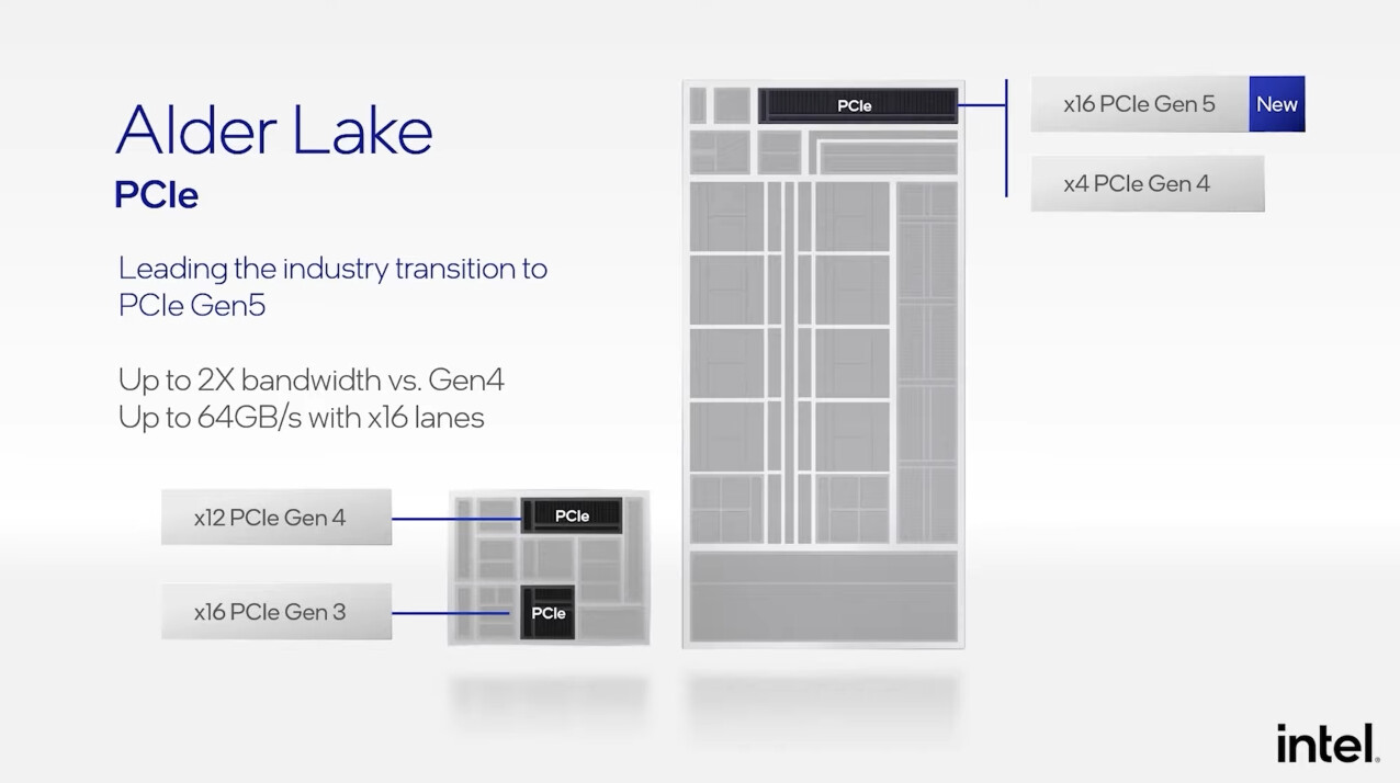
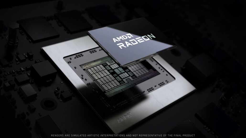
New Specs of AMD RDNA3 GPUs Emerge

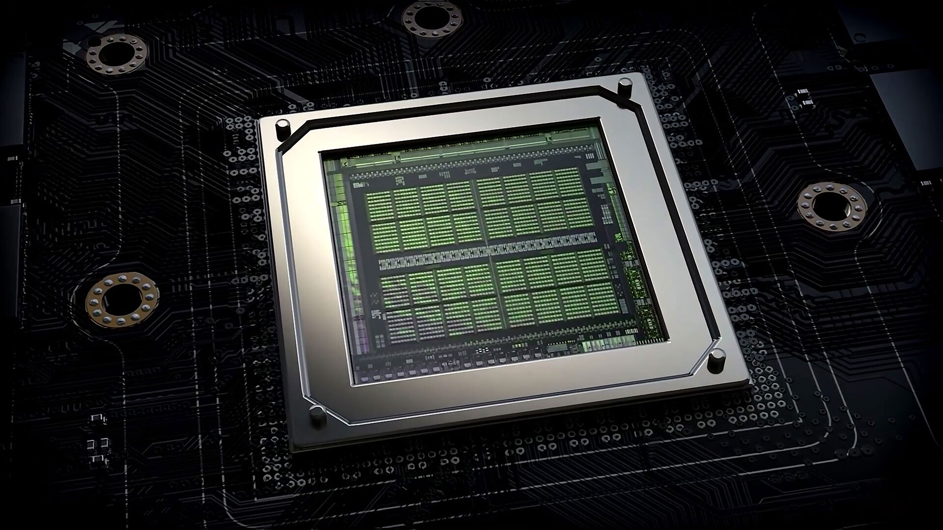
A new list of specifications of AMD's next-generation "Navi 3x" GPUs based on the RDNA3 graphics architecture emerged, with lower CU counts than previously reported. It turns out that the large "Navi 31" GPU comes with 12,288 stream processors across 48 WGP (workgroup processors), 12 SA (shader arrays), and 6 SE (shader engines). This still amounts to a 140% increase in stream processors over the Navi 21. This chip will power SKUs that succeed the Radeon RX 6800-series and RX 6900-series.

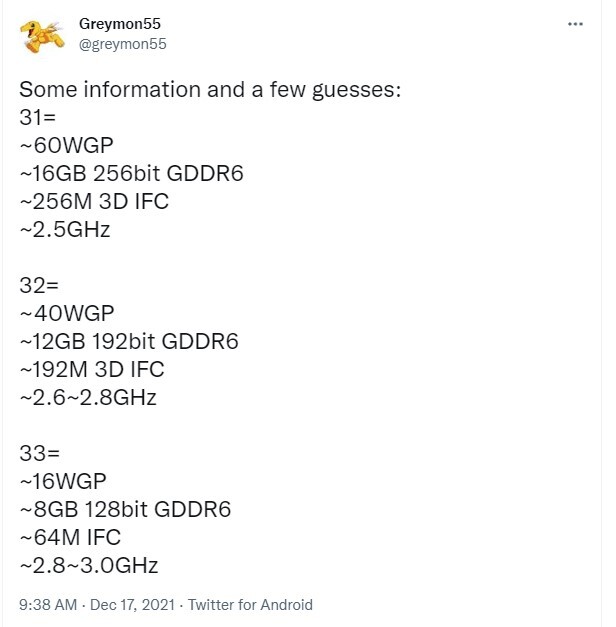
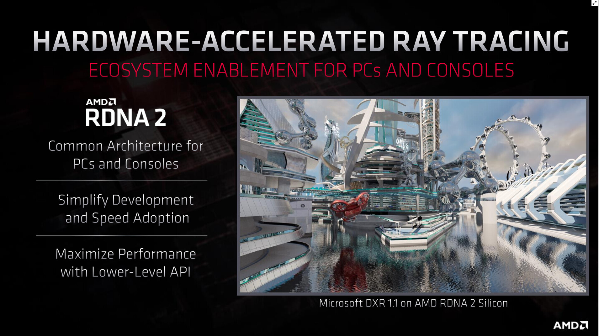
The second largest silicon from the series is the Navi 32, with two-thirds the number-crunching machinery of the Navi 31. That's 8,192 stream processors across 32 WGPs, 8 SAs, and 4 SEs. The Navi 32 silicon powers successors of the RX 6700-series. The third largest chip is the Navi 33, with half the muscle of the Navi 32, and one-third that of the Navi 31. This means 4,096 stream processors spread across 16 WGP, 4 SA, and 2 SE. There's no word on other specs such as memory bus width, but we've heard rumors of AMD doubling down on the Infinity Cache memory technology, by giving these chips even larger on-die caches. RDNA3 is also expected to improve ray tracing performance, as more of the ray tracing pipeline is handled by fixed-function hardware.

NVIDIA AD102 and AMD Navi 31 in a Race to Reach 100 TFLOPs FP32 First

A technological race is brewing between NVIDIA and AMD over which brand's GPU reaches the 100 TFLOP/s peak FP32 throughput mark first. AMD's TeraScale graphics architecture and the "RV770" silicon, were the first to hit the 1 TFLOP/s mark, way back in 2008. It would take 14 years for this figure to reach 100 TFLOP/s for flagship GPUs. NVIDIA's next generation big GPU based on the "Ada Lovelace," the AD102, is the green team's contender for the 100 TFLOP/s mark, according to kopite7kimi. To achieve this, all 144 streaming multiprocessors (SM) or 18,432 CUDA cores, of the AD102 will have to be enabled.

From the red team, the biggest GPU based on the next-generation RDNA3 graphics architecture, "Navi 31," could offer peak FP32 throughput of 92 TFLOP/s according to greymon55, which gives AMD the freedom to create special SKUs running at high engine clocks, just to reach the 100 TFLOP/s mark. The Navi 31 silicon is expected to triple the compute unit count over its predecessor, resulting in 15,360 stream processors. Both the AD102 and Navi 31 are expected to be built on the same TSMC N5 (5 nm EUV) node, and product launches for both are expected by year-end.

"Navi 31" RDNA3 Sees AMD Double Down on Chiplets: As Many as 7

Way back in January 2021, we heard a spectacular rumor about "Navi 31," the next-generation big GPU by AMD, being the company's first logic-MCM GPU (a GPU with more than one logic die). The company has a legacy of MCM GPUs, but those have been a single logic die surrounded by memory stacks. The RDNA3 graphics architecture that the "Navi 31" is based on, sees AMD fragment the logic die into smaller chiplets, with the goal of ensuring that only those specific components that benefit from the TSMC N5 node (6 nm), such as the number crunching machinery, are built on the node, while ancillary components, such as memory controllers, display controllers, or even media accelerators, are confined to chiplets built on an older node, such as the TSMC N6 (6 nm). AMD had taken this approach with its EPYC and Ryzen processors, where the chiplets with the CPU cores got the better node, and the other logic components got an older one.

Greymon55 predicts an interesting division of labor on the "Navi 31" MCM. Apparently, the number-crunching machinery is spread across two GCD (Graphics Complex Dies?). These dies pack the Shader Engines with their RDNA3 compute units (CU), Command Processor, Geometry Processor, Asynchronous Compute Engines (ACEs), Rendering Backends, etc. These are things that can benefit from the advanced 5 nm node, enabling AMD to the CUs at higher engine clocks. There's also sound logic behind building a big GPU with two such GCDs instead of a single large GCD, as smaller GPUs can be made with a single such GCD (exactly why we have two 8-core chiplets making up a 16-core Ryzen processors, and the one of these being used to create 8-core and 6-core SKUs). The smaller GCD would result in better yields per wafer, and minimize the need for separate wafer orders for a larger die (such as in the case of the Navi 21).

AMD to Refresh the Radeon RX 6000 Desktop Series with Faster Memory

AMD is preparing a round of updates to its desktop Radeon RX 6000 series in the wake of RTX 30-series models by NVIDIA, according to Greymon55, a reliable source with GPU rumors. The company could be leveraging faster 18 Gbps GDDR6 memory chips for the task. This wouldn't be the first RX 6000 series products with 18 Gbps memory, as the liquid-cooled MBA (made-by-AMD) RX 6900 XT that's exclusive to OEMs, already comes with 18 Gbps memory clocks.

Mass-production of JEDEC-standard GDDR6 memory chips with data-rates as high as 20 Gbps and 24 Gbps by Samsung is expected to get underway later this year. The company is already sampling these chips, and it's likely that they may feature in the next round of product-stack updates by AMD and NVIDIA. In the run up to its next-gen RDNA3 graphics architecture, AMD is rumored to be working on a refresh of RDNA2 on the new TSMC N6 (6 nm) foundry node that it already leverages for the entry-level "Navi 24" ASIC. This is expected to open up headroom to dial up engine clocks, and possibly support faster memory. As for this latest refresh with 18 Gbps memory, if AMD's naming convention for its mobile RX 6850M is anything to go by, the new SKUs could feature a similar "xx50" model numbering.

AMD Radeon "Navi 3x" Could See 50% Increase in Shaders, Double the Cache Memory

AMD's next generation Radeon "Navi 3x" line of GPUs could see a 50% increase in shaders and a doubling Infinity Cache memory size, according to some educated-guesswork and intelligence by Greymon55, a reliable source with GPU leaks. The Navi 31, Navi 32, and Navi 33 chips are expected to debut the new RDNA3 graphics architecture, and succeed the 6 nm optical-shrinks of existing Navi 2x chips that AMD is rumored to be working on.

The top Navi 31 part allegedly features 60 workgroup processors (WGPs), or 120 compute units. Assuming an RDNA3 CU still holds 64 stream processors, you're looking at 7,680 stream processors, a 50% increase over Navi 21. The Navi 32 silicon features 40 WGPs, and exactly the same number of shaders as the current Navi 21, at 5,120. The smallest of the three, the Navi 33, packs 16 WGPs, or 2,048 shaders. There is a generational doubling in cache memory, with 256 MB on the Navi 31, 192 MB on the Navi 32, and 64 MB on the Navi 33. Interestingly, the memory sizes and bus widths are unchanged, but AMD could leverage faster GDDR6 memory types. 2022 will see the likes of Samsung ship GDDR6 chips with data-rates as high as 24 Gbps.

Intel's "Alder Lake" Desktop Processor supports DDR4+DDR5, (only few) PCIe Gen 5 and Dynamic Memory Clock

Intel will beat AMD to next-generation I/O, with its 12th Generation Core "Alder Lake-S" desktop processors. The company confirmed that the processor will debut both DDR5 memory and PCI-Express Gen 5.0, which double data-rates over current-gen DDR4 and PCI-Express Gen 4, respectively. "Alder Lake-S" features a dual-channel DDR5 memory interface, with data-rates specced to DDR5-4800 MHz, more with overclocking, reaching enthusiast-grade memory attaining speeds in excess of DDR5-7200. Besides speed, DDR5 is expected to herald a doubling in density, with 16 GB single-rank modules becoming a common density-class, 32 GB single-rank being possible in premium modules; and 64 GB dual-rank modules being possible soon. Leading memory manufacturers have started announcing their first DDR5 products in preparation of "Alder Lake-S" launch in Q4-2021.

The memory controller is now able to dynamically adjust memory frequency and voltage, depending on current workload, power budget and other inputs—a first for the PC! This could even mean automatic "Turbo" overclocking for memory. Intel also mentioned "Enhanced Overclocking Support" but didn't go into further detail what that entails. While DDR5 is definitely the cool new kid on the block, Intel's Alder Lake memory controller keeps support for DDR4, and LPDDR4, while adding LPDDR5-5200 support (important for mobile devices). Just to clarify, there won't be one die support DDR5, and another for DDR4, no, all dies will have support for all four of these memory standards. How that will work out for motherboard designs is unknown at this point.

AMD Radeon RX 7000 Series to Include 6nm Optical-Shrinks of RDNA2

AMD's upcoming Radeon RX 7000 series could include GPUs from both the RDNA3 and RDNA2 graphics architectures, according to reliable sources on social media. This theory holds that the company could introduce new 5 nm GPUs based on the new RDNA3 architecture for the higher end, namely the Navi 31 and Navi 32; while giving the current-gen RDNA2 architecture a new lease of life in the lower segments. This isn't, however, a simple rebrand.

Apparently, some existing Navi 2x series chips will receive an optical shrink to the 6 nm node, in a bid to improve their performance/Watt. Some of the performance/Watt improvement could be used to increase engine clocks. These include the Navi 22, with its 40 RDNA2 compute units and 192-bit GDDR6 memory bus; and the Navi 23, with its 32 RDNA2 compute units and 128-bit GDDR6 memory bus. The updated Navi 22 will power the SKU that succeeds the current RX 6600 XT, while the updated Navi 23 works the lower-mainstream SKU RX x500-class.

DisplayPort 2.0 Could Land in Next-Generation AMD Radeon RDNA3 GPUs

AMD is slowly preparing to launch its next-generation of graphics cards based on the RDNA3 architecture, and it could bring some new connectivity options as well. Currently, the graphics cards we are using today use DisplayPort 1.4 connector for their DP output. However, the more advanced DisplayPort 2.0 could land in RDNA3 GPUs, bringing much-needed improvements to the video output system. What DP 2.0 brings to the table is an upgrade to an Ultra High Bit Rate individual lane speed of 20 GB/s, totaling 80 GB/s with four of those. The DP 2.0 capable system would be able to output a 10K uncompressed resolution at 60 Hz, or two 4K 144 Hz monitors at the same time. With compression, that would be extended much further. We have to wait and see what AMD does and if the next-generation RDNA3 brings this new DisplayPort standard to the masses.

AMD Stock Breaks $100 Price, Slightly Up from $7 Prior to Zen Breakthrough in 2017

As of 16:11 UTC today (29/07), the AMD stock has broken through the $100 stock-price glass ceiling, and is at $103.91, up 1384% from the $7 stock price in late-2016, prior to the company's competitive breakthrough with the "Zen" architecture. The latest rally comes in the wake of AMD's latest Q2-2021 financial results, where it clocked a 99% growth in YoY revenue. In the call, AMD mentioned that it is on track to maintaining its performance leadership, on the backs of the new "Zen 4" CPU architecture, RDNA3 graphics-, and CDNA2 compute architecture.

AMD Zen 4 and RDNA3 Confirmed for 2022, Zen 3 Refresh

AMD CEO Dr Lisa Su, in the company's Q2-2021 financial results call, confirmed that the company is on-track to launch the Zen 4 CPU microarchitecture and RDNA3 graphics architecture, in 2022. Zen 4 would herald the first major desktop platform change since the original Zen architecture, with the introduction of a new CPU socket, and support for DDR5 memory. The RDNA3 graphics architecture, meanwhile, is expected to nearly triple SIMD resources over the previous generation, and introduce even more fixed-function hardware for raytracing.

In the meantime, AMD is preparing a counter to Intel's 12th Gen Core "Alder Lake-S" processor, in the form of Zen 3 with 3D Vertical Cache, which is also being referred to as the Zen 3+ architecture. These processors feature additional last-level cache, and the company claims a 15% gaming performance uplift, which should help it close the gaming performance gap with Intel, and win on sheer core-count of its big cores. It remains to be seen if Zen 3+ remains on Socket AM4 or if it debuts AM5, as AMD will be under pressure to match "Alder Lake" in platform I/O, which includes DDR5. Dr Su also confirmed that AMD has started shipping the Instinct MI200 "Aldebaran" compute accelerator based on the CDNA2 architecture. AMD's first MCM GPU with two logic dies, "Aldebaran" takes the fight to NVIDIA's top A100 series compute accelerators, and has already scored wins with ongoing HPC/supercomputing projects.

Next-Gen AMD Radeon RDNA3 Flagship To Feature 15,360 Stream Processors?

AMD's next generation RDNA3 graphics architecture generation could see a near-quadrupling in raw SIMD muscle over the current RDNA2, according to a spectacular rumor. Apparently, the company will deploy as many as 15,360 stream processors (quadruple that of a Radeon RX 6800), and spread across 60 WGPs (Workgroup Processors), and do away with the compute unit. This is possibly because the RDNA3 compute unit won't be as independent as the ones on the original RDNA or even RDNA2, which begins to see groups of two CUs share common resources.

Another set of rumors suggest that AMD won't play NVIDIA's game of designing GPUs with wide memory bus widths, and instead build on its Infinity Cache technology, by increasing the on-die cache size and bandwidth, while retaining "affordable" discrete memory bus widths, such as 256-bit. As for the chip itself, it's rumored that the top RDNA3 part, the so-called "Navi 31," could feature a multi-chip module design (at least two logic dies), each with 30 WGPs. Each of the two is expected to be built on a next-gen silicon fabrication node that's either TSMC N5 (5 nm), or a special 6 nm node TSMC is designing for AMD. Much like the next-generation "Lovelace" architecture by NVIDIA, AMD's RDNA3 could see the light of the day only in 2022.

AMD Zen 4 and RDNA3 Architectures Launching Around the Same Time in 2022

AMD is expected to debut its next-generation "Zen 4" microarchitecture and RDNA3 graphics architectures around the same time, in 2022, according to internal company roadmaps seen by Broly_X1 on Twitter, who has leaked AMD roadmaps before. The "Zen 4" microarchitecture in particular sees AMD debut processors based on the 5 nm silicon fabrication process, and the company's first implementation of an EUV node. With "Zen 4" in 2022, the company could target a so-called "Zen 3+" microarchitecture launch later in 2021, which combines the "Zen 3" CCD with 64 MB of 3D Vertical Cache, a feature that enables a 15% gaming performance uplift, the company claims.

The RDNA3 graphics architecture could see a greater deal of effort toward improving real-time raytracing performance, with more fixed-function hardware dedicated to raytracing. The architecture could see an even bigger generational performance uplift than the one seen between RDNA and RDNA2, according to a PCGamesN report. Across the fence, "Zen 4" and RDNA3 will be squaring off against Intel's "Meteor Lake" and NVIDIA's "ADA Lovelace" architectures, respectively. RDNA3 finishes tape-out toward the end of 2021, as the 5 nm EUV node is already available to AMD for prototyping.

AMD Patents Chiplet Architecture for Radeon GPUs

On December 31st, AMD's Radeon group has filed a patent for a chiplet architecture of the GPU, showing its vision about the future of Radeon GPUs. Currently, all of the GPUs available on the market utilize the monolithic approach, meaning that the graphics processing units are located on a single die. However, the current approach has its limitations. As the dies get bigger for high-performance GPU configurations, they are more expensive to manufacture and can not scale that well. Especially with modern semiconductor nodes, the costs of dies are rising. For example, it would be more economically viable to have two dies that are 100 mm² in size each than to have one at 200 mm². AMD realized that as well and has thus worked on a chiplet approach to the design.

AMD reports that the use of multiple GPU configuration is inefficient due to limited software support, so that is the reason why GPUs were kept monolithic for years. However, it seems like the company has found a way to go past the limitations and implement a sufficient solution. AMD believes that by using its new high bandwidth passive crosslinks, it can achieve ideal chiplet-to-chiplet communication, where each GPU in the chiplet array would be coupled to the first GPU in the array. All the communication would go through an active interposer which would contain many layers of wires that are high bandwidth passive crosslinks. The company envisions that the first GPU in the array would communicably be coupled to the CPU, meaning that it will have to use the CPU possibly as a communication bridge for the GPU arrays. Such a thing would have big latency hit so it is questionable what it means really.

AMD Looks to Keep Performance, Efficiency Gains Momentum With Zen 4, RDNA 3, and Commitment to Threadripper

AMD's Executive Vice President Rick Bergman in an interview with The Street shed some light on the company's future plans for Zen 4 and RDNA 3, even as we are still reeling from (or coming in to) Zen 3 and RDNA 2's launches. Speaking on RDNA 3, Rick Bergman mentioned the company's commitment to achieve the same 50% performance-per-watt increase they achieved with RDNA 2, and had some interesting takes on the matter of why this is actually one of the most important metrics:
Rick BergmanIt just matters so much in many ways, because if your power is too high -- as we've seen from our competitors -- suddenly our potential users have to buy bigger power supplies, very advanced cooling solutions. And in a lot of ways, very importantly, it actually drives the [bill of materials] of the board up substantially. This is a desktop perspective. And invariably, that either means the retail price comes up, or your GPU cost has to come down. We focused on that for RDNA 2. It's a big focus on RDNA 3 as well.

Huawei's Loss AMD's Gain, TSMC Develops Special 5nm Node

With Mainland Chinese tech giant Huawei being effectively cut off from contracting Taiwanese TSMC to manufacture its next-generation HiSilicon 5G mobile SoCs, and NVIDIA switching to Samsung for its next-generation GPUs, TSMC is looking to hold on to large high-volume customers besides Apple and Qualcomm, so as to not let them dictate pricing. AMD is at the receiving end of the newfound affection, with the semiconductor firm reportedly developing a new refinement of its 5 nm node specially for AMD, possibly to make Sunnyvale lock in on TSMC for its future chip architectures. A ChainNews report decoded by @chiakokhua sheds light on this development.

AMD is developing its "Zen 4" CPU microarchitecture for a 5 nm-class silicon fabrication node, although the company doesn't appear to have zeroed in on a node for its RDNA3 graphics architecture and CDNA2 scalar compute architecture. In its recent public reveal of the two, AMD chose not to specify the foundry node for the two, which come out roughly around the same time as "Zen 4." It wouldn't be far fetched to predict that AMD and TSMC were waiting on certainty for the new 5 nm-class node's development. There are no technical details of this new node. AMD's demand for TSMC is expected to be at least 20,000 12-inch wafers per month.

AMD "Zen 4" Microarchitecture On Track for 2021-22 Debut with "Genoa"

AMD's 4th generation EPYC line of enterprise processors, now into design stage, impressed the United States Department of Energy enough that it wants to deploy it in "El Capitan," a 2 ExaFLOP supercomputer that will be the world's most powerful, when it goes online around 2022. Codenamed "Genoa," 4th gen EPYC implements AMD's "Zen 4" microarchitecture. While AMD didn't get into too many details about it in its 2020 Financial Analyst Day address, there are a couple of details.

For starters, "Zen 4" continues on AMD's trajectory of adding IPC gains with each generation. Secondly, "Zen 4" will leverage the advanced 5 nm silicon fabrication process, which should significantly increase transistor densities over even the most advanced iterations of 7 nm, such as 7 nm EUV. "Zen 4" comes out roughly the same time as the RDNA3 and CDNA2 graphics architectures, and AMD's 3rd generation Infinity Fabric interconnect that enables exascale supercomputers thanks to coherent unified memory and vast shared memory pools between CPUs and compute GPUs. Elsewhere in the roadmap, we see AMD announcing that its upcoming "Zen 3" microarchitecture and its enterprise implementation, the EPYC "Milan" processor, will release only toward the end of 2020. This would give EPYC "Rome" close to 6 calendar quarters of market leadership.

AMD RDNA2 Graphics Architecture Detailed, Offers +50% Perf-per-Watt over RDNA

With its 7 nm RDNA architecture that debuted in July 2019, AMD achieved a nearly 50% gain in performance/Watt over the previous "Vega" architecture. At its 2020 Financial Analyst Day event, AMD made a big disclosure: that its upcoming RDNA2 architecture will offer a similar 50% performance/Watt jump over RDNA. The new RDNA2 graphics architecture is expected to leverage 7 nm+ (7 nm EUV), which offers up to 18% transistor-density increase over 7 nm DUV, among other process-level improvements. AMD could tap into this to increase price-performance by serving up more compute units at existing price-points, running at higher clock speeds.

AMD has two key design goals with RDNA2 that helps it close the feature-set gap with NVIDIA: real-time ray-tracing, and variable-rate shading, both of which have been standardized by Microsoft under DirectX 12 DXR and VRS APIs. AMD announced that RDNA2 will feature dedicated ray-tracing hardware on die. On the software side, the hardware will leverage industry-standard DXR 1.1 API. The company is supplying RDNA2 to next-generation game console manufacturers such as Sony and Microsoft, so it's highly likely that AMD's approach to standardized ray-tracing will have more takers than NVIDIA's RTX ecosystem that tops up DXR feature-sets with its own RTX feature-set.
AMD GPU Architecture Roadmap RDNA2 RDNA3 AMD RDNA2 Efficiency Roadmap AMD RDNA2 Performance per Watt AMD RDNA2 Raytracing

AMD Financial Analyst Day 2020 Live Blog

AMD Financial Analyst Day presents an opportunity for AMD to talk straight with the finance industry about the company's current financial health, and a taste of what's to come. Guidance and product teasers made during this time are usually very accurate due to the nature of the audience. In this live blog, we will post information from the Financial Analyst Day 2020 as it unfolds.
20:59 UTC: The event has started as of 1 PM PST. CEO Dr Lisa Su takes stage.
Return to Keyword Browsing
May 15th, 2024 20:58 EDT change timezone

New Forum Posts

Popular Reviews

Controversial News Posts