Monday, January 20th 2014

AMD A10-7700K "Kaveri" De-lidded
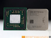
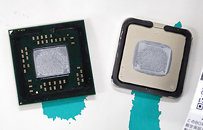
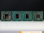
Here are the first pictures of an AMD A10-7700K "Kaveri" APU with its integrated heat-spreader (IHS, or 'lid') removed. Put next to its predecessors, "Richland," "Trinity," and "Llano," AMD's new APU silicon is its biggest for the DIY PC market, more so because it's built on the 28 nm silicon fab process, compared to its predecessors being built on 32 nm. The die measures roughly 245 mm², and packs a staggering 2.41 billion transistors.
Under the IHS, AMD is using a thermal paste to transport heat from the die, and not a solder. The chip should be easy to de-lid, if you know what you're doing. Kaveri integrates two "Steamroller" x86-64 CPU modules with two cores each, a total of 4 MB of L2 cache, a massive on-die GPU with 512 stream processors based on the Graphics CoreNext micro-architecture, a dual-channel DDR3 IMC with hUMA and DDR3-2400 native support; and a PCI-Express 3.0 root complex.
Source:
Akiba PC Hotline
Under the IHS, AMD is using a thermal paste to transport heat from the die, and not a solder. The chip should be easy to de-lid, if you know what you're doing. Kaveri integrates two "Steamroller" x86-64 CPU modules with two cores each, a total of 4 MB of L2 cache, a massive on-die GPU with 512 stream processors based on the Graphics CoreNext micro-architecture, a dual-channel DDR3 IMC with hUMA and DDR3-2400 native support; and a PCI-Express 3.0 root complex.


27 Comments on AMD A10-7700K "Kaveri" De-lidded
Be sure to read up on it, first.