Wednesday, November 16th 2016

Samsung, TSMC, AMD and Intel at ISSCC: 7nm SRAM, ZEN and Altera FPGAs detailed
The International Solid State Circuits Conference (ISSCC) is around the corner, and that means that some of the biggest players (and greatest minds) behind these particular pieces of technology will be in attendance. The annual event will gather about 3,000 engineers in February to share state-of-the-art work across a wide range of logic and memory chips.
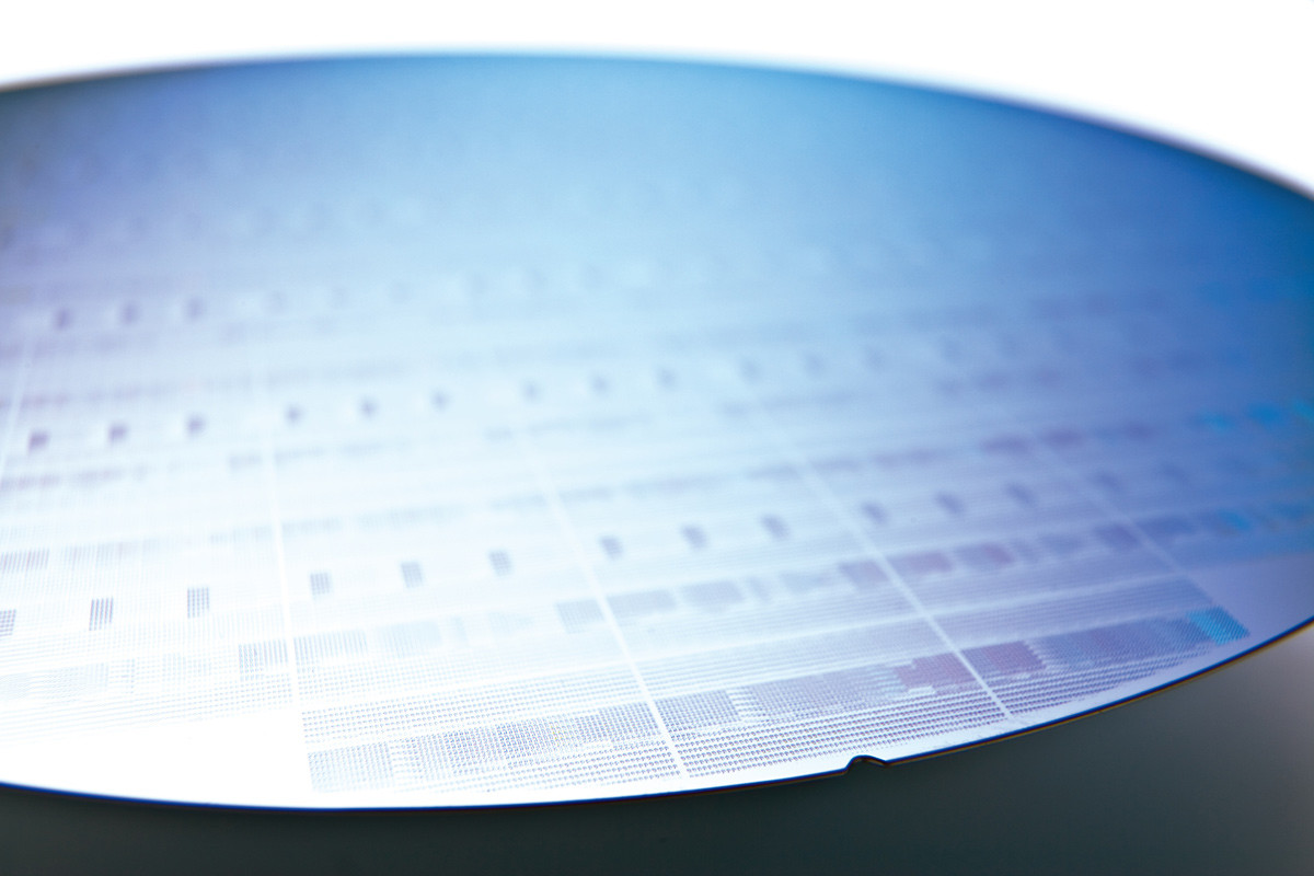
At a time when progress in traditional chip scaling is slowing down (with continued reports regarding the death of Moore's law, at least in regard to currently-used manufacturing techniques and materials), Samsung and TSMC will describe 7nm SRAMs. In general-purpose processors, AMD will give an in-depth look at its upcoming Zen x86 core, and Intel will detail its Altera Stratix 10 FPGA. In memories, Samsung and a team of Western Digital and Toshiba will show competing 512 Gbit 3-D NAND flash chips.

 TSMC is expected to unveil the smallest SRAM bit cell published to date: at 0.027mm2, a 256 Mbit SRAM chip is made in a 7nm FinFET process using write-assist circuitry for low Vmin applications. Samsung, however, will not be far behind, presenting a 7nm FinFET SRAM less than 0.030mm² in area. Interestingly, the part is made using extreme ultraviolet lithography - a technology expected to allow further reductions in production scales, but rendered extremely, technically difficult to achieve. That said, Samsung announced earlier this year it plans to put EUV steppers into production earlier than rivals, in part because it is testing them in both logic and memory fabs, whereas TSMC has said it will wait for 5nm before inserting EUV.
Separately, researchers will give keynote talks on the state of two emerging technologies expected to have broad impact -- DNA sequencing and quantum computing, while Mediatek will show a more conventional 10nm SoC and STMicroelectronics will unveil a neural network accelerator made in a fully depleted silicon-on-insulator process. Also, two keynotes at ISSCC will explore emerging ways to advance semiconductors with chip stacks, novel circuit designs and new materials.
At a time when progress in traditional chip scaling is slowing down (with continued reports regarding the death of Moore's law, at least in regard to currently-used manufacturing techniques and materials), Samsung and TSMC will describe 7nm SRAMs. In general-purpose processors, AMD will give an in-depth look at its upcoming Zen x86 core, and Intel will detail its Altera Stratix 10 FPGA. In memories, Samsung and a team of Western Digital and Toshiba will show competing 512 Gbit 3-D NAND flash chips.


Separately, researchers will give keynote talks on the state of two emerging technologies expected to have broad impact -- DNA sequencing and quantum computing, while Mediatek will show a more conventional 10nm SoC and STMicroelectronics will unveil a neural network accelerator made in a fully depleted silicon-on-insulator process. Also, two keynotes at ISSCC will explore emerging ways to advance semiconductors with chip stacks, novel circuit designs and new materials.
9 Comments on Samsung, TSMC, AMD and Intel at ISSCC: 7nm SRAM, ZEN and Altera FPGAs detailed
Hopefully we get even more information about Zen, and 7nm SRAM becomes a reality and we get bigger, faster caches.
I don't see what the big deal is. Intel probably has multiple moles feeding them everything. Even just a few hard numbers would prevent lots of people from buying skylake right now (assuming it's up to snuff).
IE, fixed :p