8
Cores
16
Threads
35 W
TDP
3.8 GHz
Frequency
5.1 GHz
Boost
Phoenix
Codename
Socket FP8
Socket
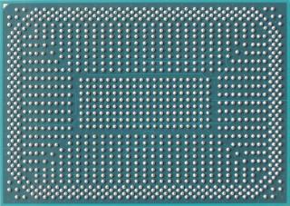
The AMD Ryzen 7 7840H is a mobile processor with 8 cores, launched in January 2023. It is part of the Ryzen 7 lineup, using the Zen 4 (Phoenix) architecture with Socket FP8. Thanks to AMD Simultaneous Multithreading (SMT) the core-count is effectively doubled, to 16 threads. Ryzen 7 7840H has 16 MB of L3 cache and operates at 3.8 GHz by default, but can boost up to 5.1 GHz, depending on the workload. AMD is building the Ryzen 7 7840H on a 4 nm production process using 25,000 million transistors. The silicon die of the chip is not fabricated at AMD, but at the foundry of TSMC. The multiplier is locked on Ryzen 7 7840H, which limits its overclocking capabilities.
With a TDP of 35 W, the Ryzen 7 7840H consumes only little energy. AMD's processor supports DDR5 memory with a dual-channel interface. The highest officially supported memory speed is 5600 MT/s, but with overclocking (and the right memory modules) you can go even higher. ECC memory is supported, too, which is an important capability for mission-critical systems, to avoid data corruption. For communication with other components in the system, Ryzen 7 7840H uses a PCI-Express Gen 4 connection. This processor features the Radeon 780M integrated graphics solution.
Hardware virtualization is available on the Ryzen 7 7840H, which greatly improves virtual machine performance. Programs using Advanced Vector Extensions (AVX) will run on this processor, boosting performance for calculation-heavy applications. Besides AVX, AMD has added support for the newer AVX2 and AVX-512 instructions, too.
Physical
| Socket: | AMD Socket FP8 |
|---|---|
| Foundry: | TSMC |
| Process Size: | 4 nm |
| Transistors: | 25,000 million |
| Die Size: | 178 mm² |
| Package: | FP8, FP7, FP7r2 |
| tJMax: | 100°C |
Processor
| Market: | Mobile |
|---|---|
| Production Status: | Active |
| Release Date: | Jan 2023 |
| Part#: | 100-000000955 (FP7r2) 100-000000964 (FP7) 100-000001129 (FP8) |
Performance
| Frequency: | 3.8 GHz |
|---|---|
| Turbo Clock: | up to 5.1 GHz |
| Base Clock: | 100 MHz |
| Multiplier: | 38.0x |
| Multiplier Unlocked: | No |
| TDP: | 35 W |
| Configurable TDP: | 35-54 W |
Architecture
| Codename: | Phoenix |
|---|---|
| Generation: |
Ryzen 7
(Zen 4 (Phoenix)) |
| Memory Support: | DDR5 |
| LPDDR5x Speed: | 7500 MT/s |
| Rated Speed: | 5600 MT/s |
| Memory Bus: | Dual-channel |
| ECC Memory: | Yes |
| PCI-Express: |
Gen 4, 20 Lanes (CPU only) |
Core Config
| # of Cores: | 8 |
|---|---|
| # of Threads: | 16 |
| SMP # CPUs: | 1 |
| Integrated Graphics: | Radeon 780M |
Cache
| Cache L1: | 64 KB (per core) |
|---|---|
| Cache L2: | 1 MB (per core) |
| Cache L3: | 16 MB (shared) |
Features
|
Notes
| China market exclusive. Graphics engine boost clock: 2700MHz ECC support on FP7r2 platforms only. |
Nov 8th, 2024 13:31 EST
change timezone
Latest GPU Drivers
New Forum Posts
- Crossfire R9 Fury not available (9)
- Post your 7-Zip v22.01 scores (401)
- Asus ROG X670E Hero Chipset Temperature (11)
- What's your latest tech purchase? (22173)
- [Testers-Needed] Converting Any Realtek Ethernet to Intel Killer Ethernet chip (61)
- What are you playing? (22173)
- OPTANE p5820x 1.6 TB - Discussion (25)
- 5950x/5900x on a low end trash mb-black friday sale (42)
- I can,t get 3DMark99 or 2000 to work on 2000 (16)
- Weird cold boot issue on Crosshair Hero X670E (47)
Popular Reviews
- AMD Ryzen 7 9800X3D Review - The Best Gaming Processor
- MSI MPG X870E Carbon Wi-Fi Review
- Dragon Age: The Veilguard Performance Benchmark Review
- NuPhy Air60 HE Review - World's First Low Profile Magnetic Keyboard
- Dragon Age: The Veilguard Handheld Performance Review
- Upcoming Hardware Launches 2024 (Updated Nov 2024)
- ECS LIVA Z7 Plus Barebone Mini-PC (Intel Core Ultra 5 125H) Review
- SilverStone SETA A2 Review
- Intel Core Ultra 9 285K Review
- Darmoshark M5 Review
Controversial News Posts
- AMD Falling Behind: Radeon dGPUs Absent from Steam's Top 20 (221)
- Quick Denuvo DRM Cracks Cost Game Publishers 20% in Revenue, According to Study (136)
- AMD Introduces Next-Generation AMD Ryzen 7 9800X3D Processor, $479, Nov 7 (124)
- Apple and Samsung in the Fray to Acquire Intel: Rumor (123)
- MSI OCLab Reveals Ryzen 9000X3D 11-13% Faster Than 7000X3D, AMD Set to Dominate "Arrow Lake" in Gaming (123)
- AMD Ryzen 7 9800X3D Comes with 120W TDP, 5.20 GHz Boost, All Specs Leaked (120)
- Microsoft Offers $30 Windows 10 Security Extension for Home Users (118)
- NVIDIA Tunes GeForce RTX 5080 GDDR7 Memory to 32 Gbps, RTX 5070 Launches at CES (112)


