 / Ryzen 9")
16
Cores
32
Threads
55 W
TDP
2.5 GHz
Frequency
5.4 GHz
Boost
Fire Range
Codename
Socket FL1
Socket
Front

Connectivity

AMD Socket FL1
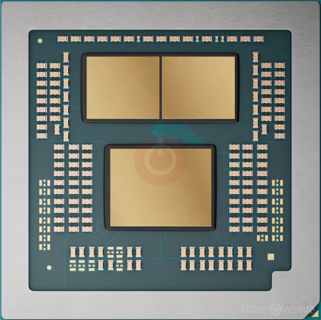
The AMD Ryzen 9 9955HX3D is a mobile processor with 16 cores, launched in January 2025. It is part of the Ryzen 9 lineup, using the Zen 5 (Fire Range) architecture with Socket FL1. Thanks to AMD Simultaneous Multithreading (SMT) the core-count is effectively doubled, to 32 threads. Ryzen 9 9955HX3D has 128 MB of L3 cache and operates at 2.5 GHz by default, but can boost up to 5.4 GHz, depending on the workload. AMD is making the Ryzen 9 9955HX3D on a 4 nm production node using 16,630 million transistors. The silicon die of the chip is not fabricated at AMD, but at the foundry of TSMC. You may freely adjust the unlocked multiplier on Ryzen 9 9955HX3D, which simplifies overclocking greatly, as you can easily dial in any overclocking frequency.
With a TDP of 55 W, the Ryzen 9 9955HX3D consumes typical power levels for a modern PC. AMD's processor supports DDR5 memory with a dual-channel interface. The highest officially supported memory speed is 5600 MT/s. ECC memory is supported, too, which is an important capability for mission-critical systems, to avoid data corruption. For communication with other components in the system, Ryzen 9 9955HX3D uses a PCI-Express Gen 5 connection. This processor features the Radeon 610M integrated graphics solution.
Hardware virtualization is available on the Ryzen 9 9955HX3D, which greatly improves virtual machine performance. Programs using Advanced Vector Extensions (AVX) can run on this processor, boosting performance for calculation-heavy applications. Besides AVX, AMD has added support for the newer AVX2 and AVX-512 instructions, too.
Physical
| Socket: | AMD Socket FL1 |
|---|---|
| Foundry: | TSMC |
| Process Size: | 4 nm |
| Transistors: | 16,630 million |
| Die Size: | 2x 70.6 mm² |
| I/O Process Size: | 6 nm |
| I/O Transistors: | 3,400 million |
| I/O Die Size: | 122 mm² |
| Package: | µFC-BGAFL1 |
| tJMax: | 100°C |
Processor
| Market: | Mobile |
|---|---|
| Production Status: | Active |
| Release Date: | Jan 6th, 2025 |
| Part#: | 100-000001030 |
| Bundled Cooler: | None |
Performance
| Frequency: | 2.5 GHz |
|---|---|
| Turbo Clock: | up to 5.4 GHz |
| Base Clock: | 100 MHz |
| Multiplier: | 25.0x |
| Multiplier Unlocked: | Yes |
| TDP: | 55 W |
| Configurable TDP: | 75 W |
| PPT: | 74-101 W |
Architecture
| Codename: | Fire Range |
|---|---|
| Generation: |
Ryzen 9
(Zen 5 (Fire Range)) |
| Memory Support: | DDR5 |
| Rated Speed: | 5600 MT/s |
| Memory Bus: | Dual-channel |
| ECC Memory: | Yes |
| PCI-Express: |
Gen 5, 28 Lanes (CPU only) |
Core Config
| # of Cores: | 16 |
|---|---|
| # of Threads: | 32 |
| SMP # CPUs: | 1 |
| Integrated Graphics: | Radeon 610M |
Cache
| Cache L1: | 80 KB (per core) |
|---|---|
| Cache L2: | 1 MB (per core) |
| Cache L3: | 128 MB (shared) |
Features
|
Notes
| Radeon graphics dynamic frequency: 400-2200 MHz Level 3 cache arranged as 2x 32MB 2D cache plus 1x 64MB 3D V-Cache. ECC modes require motherboard support. |
Mar 21st, 2025 03:43 EDT
change timezone
Latest GPU Drivers
New Forum Posts
- Is RX 9070 VRAM temperature regular value or hotspot? (67)
- Choosing the Perfect Motherboard to Complete My PC Build (15)
- SLI is really not Dead if you Have a SLI rig (93)
- What else can I do to diagnose an artifacting card? (12)
- Windows 10 Vs 11, Which one too choose? (8)
- Old Gamer Memory Upgrade Worth It? (48)
- Do you prefer factory overclocked GPUs? (38)
- Deliding 7800X3D, using TG HP Heatspreader experience? (6)
- Post your Speedtest.net Speeds! (2354)
- HalfLife2 RTX Demo Is out! (262)
Popular Reviews
- ASRock Radeon RX 9070 XT Taichi OC Review - Excellent Cooling
- be quiet! Pure Base 501 LX Review
- Sapphire Radeon RX 9070 XT Nitro+ Review - Beating NVIDIA
- AMD Ryzen 9 9950X3D Review - Great for Gaming and Productivity
- Corsair SF750 750 W Review
- ASUS GeForce RTX 5070 TUF OC Review
- MSI MAG B860 Tomahawk Wi-Fi Review
- XFX Radeon RX 9070 XT Mercury OC Magnetic Air Review
- MSI GeForce RTX 5070 Gaming Trio OC Review
- ASUS Radeon RX 9070 TUF OC Review
Controversial News Posts
- NVIDIA GeForce RTX 50 Cards Spotted with Missing ROPs, NVIDIA Confirms the Issue, Multiple Vendors Affected (519)
- AMD RDNA 4 and Radeon RX 9070 Series Unveiled: $549 & $599 (260)
- AMD Mentions Sub-$700 Pricing for Radeon RX 9070 GPU Series, Looks Like NV Minus $50 Again (250)
- NVIDIA Investigates GeForce RTX 50 Series "Blackwell" Black Screen and BSOD Issues (244)
- AMD Radeon RX 9070 and 9070 XT Official Performance Metrics Leaked, +42% 4K Performance Over Radeon RX 7900 GRE (195)
- AMD Radeon RX 9070-series Pricing Leaks Courtesy of MicroCenter (158)
- MSI Doesn't Plan Radeon RX 9000 Series GPUs, Skips AMD RDNA 4 Generation Entirely (142)
- Microsoft Introduces Copilot for Gaming (123)