8
Cores
16
Threads
28 W
TDP
2000 MHz
Frequency
5 GHz
Boost
Krackan Point
Codename
Socket FP8
Socket
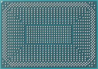
The AMD Ryzen AI 7 PRO 350 is a mobile processor with 8 cores, launched in January 2025. It is part of the Ryzen AI lineup, using the Zen 5 architecture with Socket FP8. Thanks to AMD Simultaneous Multithreading (SMT) the core-count is effectively doubled, to 16 threads. Ryzen AI 7 PRO 350 has 8 MB of L3 cache and operates at 2000 MHz by default, but can boost up to 5 GHz, depending on the workload. AMD is building the Ryzen AI 7 PRO 350 on a 4 nm production process, the transistor count is unknown. The silicon die of the chip is not fabricated at AMD, but at the foundry of TSMC. The multiplier is locked on Ryzen AI 7 PRO 350, which limits its overclocking capabilities.
With a TDP of 28 W, the Ryzen AI 7 PRO 350 consumes only little energy. AMD's processor supports DDR5 memory with a dual-channel interface. The highest officially supported memory speed is 5600 MT/s, but with overclocking (and the right memory modules) you can go even higher. ECC memory is supported, too, which is an important capability for mission-critical systems, to avoid data corruption. For communication with other components in the machine, Ryzen AI 7 PRO 350 uses a PCI-Express Gen 4 connection. This processor features the Radeon 860M integrated graphics solution.
Hardware virtualization is available on the Ryzen AI 7 PRO 350, which greatly improves virtual machine performance. Additionally, IOMMU virtualization (PCI passthrough) is supported, so that guest virtual machines may directly use host hardware. Programs using Advanced Vector Extensions (AVX) will run on this processor, boosting performance for calculation-heavy applications. Besides AVX, AMD has added support for the newer AVX2 and AVX-512 instructions, too.
Physical
| Socket: | AMD Socket FP8 |
|---|---|
| Foundry: | TSMC |
| Process Size: | 4 nm |
| Package: | FP8 |
| tJMax: | 100°C |
Processor
| Market: | Mobile |
|---|---|
| Production Status: | Active |
| Release Date: | Jan 6th, 2025 |
| Part#: | 100-000000713 |
Performance
| Frequency: | 2000 MHz |
|---|---|
| Turbo Clock: | up to 5 GHz |
| E-Core Frequency: |
2000 MHz
up to 3.5 GHz |
| Base Clock: | 100 MHz |
| Multiplier: | 20.0x |
| Multiplier Unlocked: | No |
| XDNA NPU: | 50 TOPS |
| TDP: | 28 W |
| Configurable TDP: | 15-54 W |
Architecture
| Codename: | Krackan Point |
|---|---|
| Generation: |
Ryzen AI
(Zen 5) |
| Memory Support: | DDR5 |
| LPDDR5x Speed: | 8000 MT/s |
| Rated Speed: | 5600 MT/s |
| Memory Bus: | Dual-channel |
| ECC Memory: | Yes |
| PCI-Express: |
Gen 4, 16 Lanes (CPU only) |
Core Config
| # of Cores: | 8 |
|---|---|
| # of Threads: | 16 |
| Hybrid Cores: | 3 + 5 |
| SMP # CPUs: | 1 |
| Integrated Graphics: | Radeon 860M |
Cache
| Cache L1: | 80 KB (per core) |
|---|---|
| Cache L2: | 1 MB (per core) |
| Cache L3: | 8 MB |
| E-Core L3: | 8 MB |
Features
|
Notes
| Radeon Graphics dynamic frequency: 400-3000 MHz Int8 TOPS rated at up to 66 TOPS combining CPU cores, GPU cores, and NPU. |
Jan 28th, 2025 11:10 EST
change timezone
Latest GPU Drivers
New Forum Posts
- Getting tearing in fortnite even with g-sync, framecap etc (2)
- NVidia now HIDING hot spot temperature? A great problem IMO. (107)
- Gigabyte 5090 Aorus Master VRM Specs (3)
- How many fans on a single mother board connector (0)
- AAF Optimus Modded Driver For Windows 10 & Windows 11 - Only for Realtek HDAUDIO Chips (306)
- Proposal for CPUs/graphic cards for PCs power draw standardisation (58)
- So I finally turned on HDR... (16)
- What's your latest tech purchase? (22988)
- The coffee and tea drinkers club. (208)
- E-Waste laptop repair adventures. (8)
Popular Reviews
- NVIDIA GeForce RTX 5090 Founders Edition Review - The New Flagship
- ASUS GeForce RTX 5090 Astral OC Review - Astronomical Premium
- MSI GeForce RTX 5090 Suprim Liquid SOC Review
- MSI GeForce RTX 5090 Suprim SOC Review
- NVIDIA DLSS 4 Transformer Review - Better Image Quality for Everyone
- NVIDIA GeForce RTX 5090 PCI-Express Scaling
- Palit GeForce RTX 5090 GameRock Review
- KLEVV URBANE V DDR5-7600 32 GB CL36 Review
- AMD Ryzen 7 9800X3D Review - The Best Gaming Processor
- XFX Radeon RX 7900 XTX Magnetic Air Review
Controversial News Posts
- NVIDIA 2025 International CES Keynote: Liveblog (470)
- AMD Debuts Radeon RX 9070 XT and RX 9070 Powered by RDNA 4, and FSR 4 (349)
- AMD is Taking Time with Radeon RX 9000 to Optimize Software and FSR 4 (239)
- AMD Radeon RX 9070 XT & RX 9070 Custom Models In Stock at European Stores (226)
- NVIDIA GeForce RTX 5090 Features 575 W TDP, RTX 5080 Carries 360 W TDP (217)
- New Leak Reveals NVIDIA RTX 5080 Is Slower Than RTX 4090 (200)
- AMD's Radeon RX 9070 Launch Faces Pricing Hurdles (175)
- AMD Radeon RX 9070 XT Tested in Cyberpunk 2077 and Black Myth: Wukong (169)


