2
Cores
2
Threads
65 W
TDP
3.7 GHz
Frequency
3.9 GHz
Boost
Richland
Codename
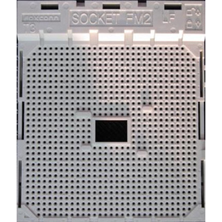
Socket FM2
Socket
The AMD A4-6300 was a desktop processor with 2 cores, launched in June 2013. It is part of the A4 lineup, using the Richland architecture with Socket FM2. A4-6300 has 1 MB of L2 cache and operates at 3.7 GHz by default, but can boost up to 3.9 GHz, depending on the workload. AMD is building the A4-6300 on a 32 nm production process using 1,303 million transistors. The multiplier is locked on A4-6300, which limits its overclocking capabilities.
With a TDP of 65 W, the A4-6300 consumes typical power levels for a modern PC. AMD's processor supports DDR3 memory with a dual-channel interface. The highest officially supported memory speed is 1600 MT/s, but with overclocking (and the right memory modules) you can go even higher. For communication with other components in the computer, A4-6300 uses a PCI-Express Gen 2 connection. This processor features the Radeon HD 8370D integrated graphics solution.
Hardware virtualization is available on the A4-6300, which greatly improves virtual machine performance. Programs using Advanced Vector Extensions (AVX) will run on this processor, boosting performance for calculation-heavy applications.
Physical
| Socket: | AMD Socket FM2 |
|---|---|
| Process Size: | 32 nm |
| Transistors: | 1,303 million |
| Die Size: | 246 mm² |
| Package: | µPGA |
| tCaseMax: | 70°C |
Processor
| Market: | Desktop |
|---|---|
| Production Status: | End-of-life |
| Release Date: | Jun 1st, 2013 |
| Part#: | AD6300OKHLBOX AD6300OKA23HL |
Performance
| Frequency: | 3.7 GHz |
|---|---|
| Turbo Clock: | up to 3.9 GHz |
| Base Clock: | 100 MHz |
| Multiplier: | 37.0x |
| Multiplier Unlocked: | No |
| Voltage: | 1.475 V |
| TDP: | 65 W |
Architecture
| Codename: | Richland |
|---|---|
| Generation: |
A4
(Richland) |
| Memory Support: | DDR3 |
| Rated Speed: | 1600 MT/s |
| Memory Bus: | Dual-channel |
| ECC Memory: | No |
| PCI-Express: | Gen 2 |
| Chipsets: | A88X, A85X, A78, A75, A68H, A55 |
Core Config
| # of Cores: | 2 |
|---|---|
| # of Threads: | 2 |
| SMP # CPUs: | 1 |
| Integrated Graphics: | Radeon HD 8370D |
Cache
| Cache L1: | 96 KB |
|---|---|
| Cache L2: | 1 MB (shared) |
Features
|
Notes
| 16KB L1 data cache per core. 64KB L1 instruction cache shared per two cores (per module). 1MB L2 cache shared per two cores (per module). |
Mar 25th, 2025 21:03 EDT
change timezone
Latest GPU Drivers
New Forum Posts
- What is the lifespan of a gaming PC motherboard? (62)
- Has anyone tried enabling FSR 4 on NVIDIA cards? (5)
- Windows 11 General Discussion (5905)
- What's your latest tech purchase? (23398)
- As we live the age of game remakes, which game you would like to see to have a remake? (372)
- Discussion: linux-6.14.X (8)
- What is going to be your next tech upgrade? just curious :) (10)
- Did Nvidia purposely gimp the performance of 50xx series cards with drivers (42)
- Build complete! Any thoughts on undervolting? (8)
- RX 9070 availability (233)
Popular Reviews
- Assassin's Creed Shadows Performance Benchmark Review - 30 GPUs Compared
- be quiet! Pure Rock Pro 3 Black Review
- ASUS ProArt X870E-Creator Wi-Fi Review
- ASRock Radeon RX 9070 XT Taichi OC Review - Excellent Cooling
- Sapphire Radeon RX 9070 XT Nitro+ Review - Beating NVIDIA
- Pulsar Feinmann F01 Review
- ASUS GeForce RTX 5070 TUF OC Review
- AMD Ryzen 9 9950X3D Review - Great for Gaming and Productivity
- AMD Ryzen 7 9800X3D Review - The Best Gaming Processor
- Montech XR Wood Review
Controversial News Posts
- AMD RDNA 4 and Radeon RX 9070 Series Unveiled: $549 & $599 (260)
- AMD Radeon RX 9070-series Pricing Leaks Courtesy of MicroCenter (158)
- MSI Doesn't Plan Radeon RX 9000 Series GPUs, Skips AMD RDNA 4 Generation Entirely (142)
- Microsoft Introduces Copilot for Gaming (123)
- AMD Radeon RX 9070 XT Reportedly Outperforms RTX 5080 Through Undervolting (118)
- NVIDIA Reportedly Prepares GeForce RTX 5060 and RTX 5060 Ti Unveil Tomorrow (115)
- Over 200,000 Sold Radeon RX 9070 and RX 9070 XT GPUs? AMD Says No Number was Given (100)
- NVIDIA GeForce RTX 5050, RTX 5060, and RTX 5060 Ti Specifications Leak (96)


