2
Cores
2
Threads
65 W
TDP
3.7 GHz
Frequency
3.9 GHz
Boost
Richland
Codename
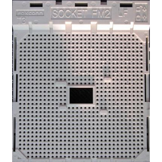
Socket FM2
Socket
The AMD A4-6300 was a desktop processor with 2 cores, launched in June 2013. It is part of the A4 lineup, using the Richland architecture with Socket FM2. A4-6300 has 1 MB of L2 cache and operates at 3.7 GHz by default, but can boost up to 3.9 GHz, depending on the workload. AMD is building the A4-6300 on a 32 nm production process using 1,303 million transistors. The multiplier is locked on A4-6300, which limits its overclocking capabilities.
With a TDP of 65 W, the A4-6300 consumes typical power levels for a modern PC. AMD's processor supports DDR3 memory with a dual-channel interface. The highest officially supported memory speed is 1600 MT/s, but with overclocking (and the right memory modules) you can go even higher. For communication with other components in the computer, A4-6300 uses a PCI-Express Gen 2 connection. This processor features the Radeon HD 8370D integrated graphics solution.
Hardware virtualization is available on the A4-6300, which greatly improves virtual machine performance. Programs using Advanced Vector Extensions (AVX) will run on this processor, boosting performance for calculation-heavy applications.
Physical
| Socket: | AMD Socket FM2 |
|---|---|
| Process Size: | 32 nm |
| Transistors: | 1,303 million |
| Die Size: | 246 mm² |
| Package: | µPGA |
| tCaseMax: | 70°C |
Processor
| Market: | Desktop |
|---|---|
| Production Status: | End-of-life |
| Release Date: | Jun 1st, 2013 |
| Part#: | AD6300OKHLBOX AD6300OKA23HL |
Performance
| Frequency: | 3.7 GHz |
|---|---|
| Turbo Clock: | up to 3.9 GHz |
| Base Clock: | 100 MHz |
| Multiplier: | 37.0x |
| Multiplier Unlocked: | No |
| Voltage: | 1.475 V |
| TDP: | 65 W |
Architecture
| Codename: | Richland |
|---|---|
| Generation: |
A4
(Richland) |
| Memory Support: | DDR3 |
| Rated Speed: | 1600 MT/s |
| Memory Bus: | Dual-channel |
| ECC Memory: | No |
| PCI-Express: | Gen 2 |
| Chipsets: | A88X, A85X, A78, A75, A68H, A55 |
Core Config
| # of Cores: | 2 |
|---|---|
| # of Threads: | 2 |
| SMP # CPUs: | 1 |
| Integrated Graphics: | Radeon HD 8370D |
Cache
| Cache L1: | 96 KB |
|---|---|
| Cache L2: | 1 MB (shared) |
Features
|
Notes
| 16KB L1 data cache per core. 64KB L1 instruction cache shared per two cores (per module). 1MB L2 cache shared per two cores (per module). |
Nov 17th, 2024 14:16 EST
change timezone
Latest GPU Drivers
New Forum Posts
- Bifurcation (2)
- whats going on with core 2 quad and windows? (19)
- Case for Gaming? (34)
- MSI monitor not working, flashing colors (2)
- TPU's Nostalgic Hardware Club (19461)
- No more driver beta testing programs (0)
- 3D Printing ideas (0)
- Upgrade from 13700k to 9800X3D (RAM issues?) (28)
- Anime Nation (12879)
- DDR5 Trident Z Royal (21)
Popular Reviews
- NVIDIA App v1.0 Review
- AMD Ryzen 7 9800X3D Review - The Best Gaming Processor
- Epomaker TH40 Wireless Mechanical Keyboard Review
- Redragon K1NG 8K Review
- Quick Look: MOONDROP Quark2 Type-C In-Ear Monitors
- Valkyrie VK02 Lite Review
- Beelink GTi12 Ultra Mini-PC + EX Dock (Intel Core i9-12900H) Review
- Upcoming Hardware Launches 2024 (Updated Nov 2024)
- Quick Look: G.SKILL WigiDash PC Command Panel
- NVIDIA GeForce RTX 4070 Super Founders Edition Review
Controversial News Posts
- AMD Falling Behind: Radeon dGPUs Absent from Steam's Top 20 (222)
- AMD Ryzen 7 9800X3D Stocks Vaporized in Retail, Being Scalped (151)
- AMD Introduces Next-Generation AMD Ryzen 7 9800X3D Processor, $479, Nov 7 (124)
- Apple and Samsung in the Fray to Acquire Intel: Rumor (123)
- AMD Ryzen 7 9800X3D Comes with 120W TDP, 5.20 GHz Boost, All Specs Leaked (120)
- Microsoft Offers $30 Windows 10 Security Extension for Home Users (118)
- AMD Ryzen 7 9800X3D Has the CCD on Top of the 3D V-cache Die, Not Under it (110)
- TechPowerUp is Hiring a Power Supply (PSU) Reviewer (105)


