Report an Error


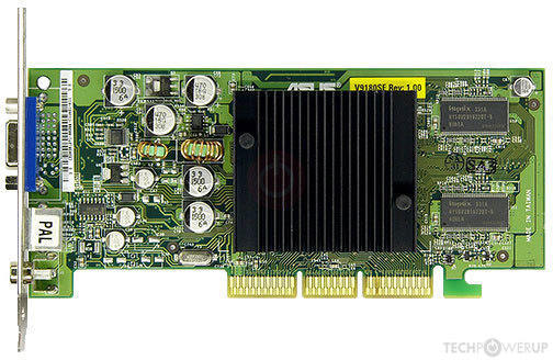
ASUS V9180 SE
- V9180SE/T/64M
- Graphics Processor
- NV18
- Pixel Shaders
- 2
- Vertex Shaders
- N/A
- TMUs
- 4
- ROPs
- 2
- Memory Size
- 64 MB
- Memory Type
- DDR
- Bus Width
- 64 bit

GPU
Graphics Processor
Graphics Card
- Release Date
- Sep 25th, 2002
- Generation
- GeForce 4 MX
- Predecessor
- GeForce 3
- Successor
- GeForce 4 Ti
- Production
- End-of-life
- Bus Interface
- AGP 8x
Clock Speeds
- GPU Clock
- 275 MHz
- Memory Clock
-
250 MHz
133 MHz (-47%)
500 Mbps effective
266 Mbps effective
Memory
- Memory Size
-
32 MB
64 MB
- Memory Type
- DDR
- Memory Bus
-
32 bit
64 bit
- Bandwidth
-
2.000 GB/s
2.128 GB/s
Render Config
- Pixel Shaders
- 2
- Vertex Shaders
- 0
- TMUs
- 4
- ROPs
- 2
Theoretical Performance
- Pixel Rate
- 550.0 MPixel/s
- Texture Rate
- 1.100 GTexel/s
Board Design
- Slot Width
- Single-slot
- TDP
- unknown
- Suggested PSU
- 200 W
- Outputs
- 1x VGA
1x S-Video
- Power Connectors
- None
Graphics Features
- DirectX
- 7.0
- OpenGL
- 1.5
- OpenCL
- N/A
- Vulkan
- N/A
- Pixel Shader
- 1.1
- Vertex Shader
- 1.1
Card Notes
| Variant Memory: 64 MB 64-bit Variant Memory: 128 MB 128-bit |
NV18 GPU Notes
| Latest Drivers: Windows NT 4: ForceWare Release 77.56 ForceWare Release 77.72 Desktop Windows 95 / 98 / ME: ForceWare Release 81.98 Latest Drivers: Windows NT 4: ForceWare Release 77.56 ForceWare Release 77.72 Desktop Windows 95 / 98 / ME: ForceWare Release 81.98 Windows 2000 / XP / Server 2003 x64: ForceWare Release 93.71 Desktop ForceWare Release 91.36 / 93.81 Beta |
Other retail boards based on this design (2)
| Name | GPU Clock | Memory Clock | Other Changes |
|---|---|---|---|
| 275 MHz | 200 MHz | 64 MB, 64 bit | |
|
ASUS V9180 SE

|
275 MHz | 133 MHz | 64 MB, 64 bit |

Jul 19th, 2024 08:20 EDT
change timezone
Latest GPU Drivers
New Forum Posts
- Include MSRP in the Specification table for every reviewed product (7)
- The TPU UK Clubhouse (25014)
- What's your latest tech purchase? (21087)
- Any other game like resident evil 1? (63)
- TPU's Nostalgic Hardware Club (18763)
- Upgrade from Acer XB271HUC IPS? (14)
- Can someone please give specs of Graphic variant 216-0867071 AMD? (2)
- Graphics card only runs with X1 instead X16 (31)
- What are you playing? (21119)
- DTS:X APO4 + DTS Interactive for Most Devices [USB Supported] (317)
Popular Reviews
- AMD Zen 5 Technical Deep Dive
- Noctua NH-D15 G2 Review - Big Performance, Bigger Price
- MCHOSE AX5 Pro Max Review
- Audeze MM-500 Open-Back Planar Magnetic Headphones Review
- Alphacool Core 1 LT CPU Water Block Review
- ID-Cooling FROZN A620 PRO SE Review - Better Value Than Thermalright
- Upcoming Hardware Launches 2024 (Updated May 2024)
- HIFIMAN Susvara Unveiled Planar Magnetic Headphones Review
- AMD Ryzen 7 7800X3D Review - The Best Gaming CPU
- The First Descendant Performance Benchmark Review - 30 GPUs Tested
Controversial News Posts
- Legendary Overclocker KINGPIN Leaves EVGA and Joins PNY to Develop Next-Generation GPUs for Extreme OC (195)
- NVIDIA GeForce RTX 50 Series "Blackwell" TDPs Leaked, All Powered by 16-Pin Connector (165)
- Noctua Announces $150 Flagship NH-D15 G2 CPU Coolers and NF-A14x25r G2 140mm Fans (164)
- Microsoft Closer to Removing Local Accounts from Windows 11, Removes Help Page on How to Switch to One (142)
- AMD is Becoming a Software Company. Here's the Plan (139)
- AMD to Revise Specs of Ryzen 7 9700X to Increase TDP to 120W, to Beat 7800X3D (112)
- Intel Planning P-core Only "Bartlett" LGA1700 Processor for 2025 (106)
- Intel "Arrow Lake-S" to See a Rearrangement of P-cores and E-cores Along the Ringbus (100)