Report an Error


ATI R200
R200

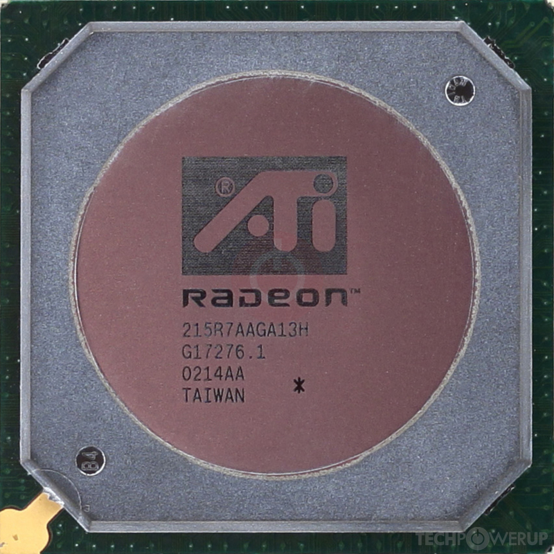
215R7AAGA13H
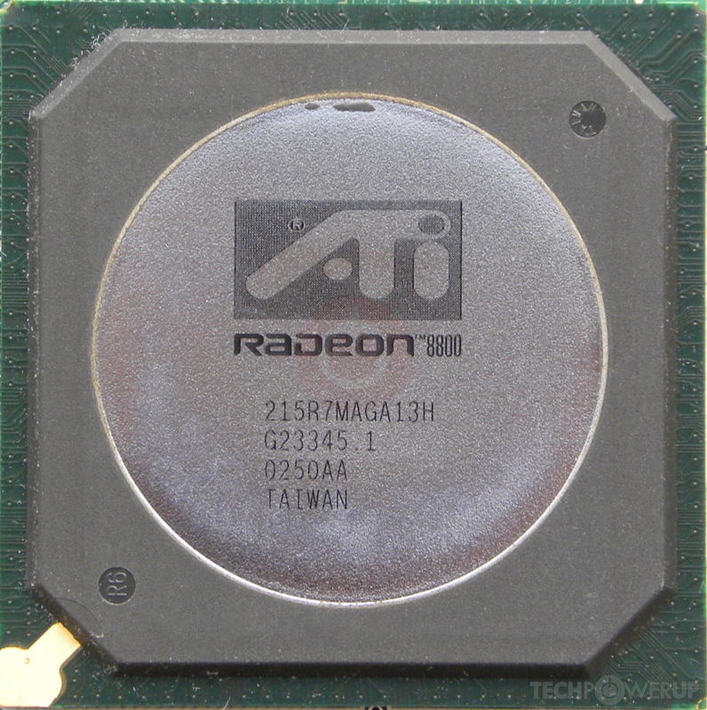
R200 GL 8800

Die Shot
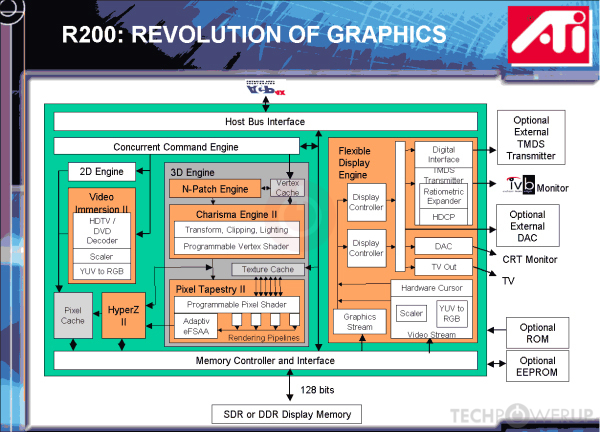
Block Diagram
ATI's R200 GPU uses the Rage 7 architecture and is made using a 150 nm production process at TSMC. With a die size of 120 mm² and a transistor count of 60 million it is a small chip. R200 supports DirectX 8.1. Modern GPU compute technologies are not available. It features 4 pixel shaders and 2 vertex shaders, 8 texture mapping units and 4 ROPs. Due to the lack of unified shaders you will not be able to run recent games at all (which require unified shader/DX10+ support).
Graphics Processor
- Released
- Aug 14th, 2001
- GPU Name
- R200
- Codename
- Chaplin
- Architecture
- Rage 7
- Foundry
- TSMC
- Process Size
- 150 nm
- Transistors
- 60 million
- Density
- 500.0K / mm²
- Die Size
- 120 mm²
Graphics Features
- DirectX
- 8.1
- OpenGL
- 1.3
- OpenCL
- N/A
- Vulkan
- N/A
- Pixel Shader
- 1.4
- Vertex Shader
- 1.1
- Compute
- GFX1
Render Config
- Pixel Shaders
- 4
- Vertex Shaders
- 2
- TMUs
- 8
- ROPs
- 4
- Max. TDP
- 92 W
All Rage 7 GPUs
ATI GPU Architecture History
Graphics cards using the ATI R200 GPU
| Name | Chip | Memory | Shaders | TMUs | ROPs | GPU Clock | Memory Clock |
|---|---|---|---|---|---|---|---|
| 215R7AAGA13H | 64 MB | 4 / 2 | 8 | 4 | 275 MHz | 275 MHz | |
| 215R7AAGA13H | 64 MB | 4 / 2 | 8 | 4 | 250 MHz | 250 MHz | |
| 64 MB | 4 / 2 | 8 | 4 | 250 MHz | 250 MHz | ||
| 64 MB | 4 / 2 | 8 | 4 | 250 MHz | 250 MHz | ||
| 64 MB | 4 / 2 | 8 | 4 | 230 MHz | 190 MHz | ||
| 128 MB | 4 / 2 | 8 | 4 | 275 MHz | 275 MHz | ||
| R200 GL 8800 | 128 MB | 4 / 2 | 8 | 4 | 300 MHz | 290 MHz | |
| R200 GL | 64 MB | 4 / 2 | 8 | 4 | 250 MHz | 270 MHz | |
| 64 MB | 4 / 2 | 8 | 4 | 250 MHz | 250 MHz |


R200 GPU Notes
| Codename: Chaplin Graphics/Compute: GFX1 Charisma Engine II Pixel Tapestry II Smart Shader 1.0 Smooth Vision 1.0 TruForm 1.0 Hyper Z Video Immersion II Programmable pixel&vertex pipelines Latest Drivers: Windows 98 / Me / 2000: Catalyst Software Suite 6.2 Windows XP: Catalyst Software Suite 6.11 |
Nov 12th, 2024 14:45 EST
change timezone
Latest GPU Drivers
New Forum Posts
- Inconsistent POSTing on PC ( already replaced multiple parts) (49)
- 9800x 3d vs 12900k - Battle of the Century (38)
- TPU's Nostalgic Hardware Club (19375)
- Performance issue w/ EVGA RTX 3090 FTW3 ULTRA V2 (3)
- What's your latest tech purchase? (22240)
- [INTEL]-How To Update Your Microcode for Intel HX 13/14th Gen. CPUs Laptops/Mobile Easily. (98)
- Different low reading (23)
- PC still rebooting randomly while gaming. (4)
- [Test Build] Fix for Driver Signing on Windows 11 24H2 (25)
- 2 sticks is better then 4 sticks? (33)
Popular Reviews
- AMD Ryzen 7 9800X3D Review - The Best Gaming Processor
- NVIDIA App v1.0 Review
- Team Group A440 Lite 2 TB Review
- FiiO Industrial Park/Factory Tour + Interview with Founder
- Upcoming Hardware Launches 2024 (Updated Nov 2024)
- ID-Cooling FX360 INF AIO Review
- MIRPH-1 Open-Back Dynamic Driver Headphones Review
- Dragon Age: The Veilguard Handheld Performance Review
- Intel Core Ultra 9 285K Review
- DDR5 Memory Performance Scaling with AMD Zen 5
Controversial News Posts
- AMD Falling Behind: Radeon dGPUs Absent from Steam's Top 20 (222)
- AMD Ryzen 7 9800X3D Stocks Vaporized in Retail, Being Scalped (140)
- Quick Denuvo DRM Cracks Cost Game Publishers 20% in Revenue, According to Study (136)
- AMD Introduces Next-Generation AMD Ryzen 7 9800X3D Processor, $479, Nov 7 (124)
- Apple and Samsung in the Fray to Acquire Intel: Rumor (123)
- AMD Ryzen 7 9800X3D Comes with 120W TDP, 5.20 GHz Boost, All Specs Leaked (120)
- Microsoft Offers $30 Windows 10 Security Extension for Home Users (118)
- AMD Ryzen 7 9800X3D Has the CCD on Top of the 3D V-cache Die, Not Under it (110)