Report an Error


ATI Rage 6
Rage 6

215R6EBGA13

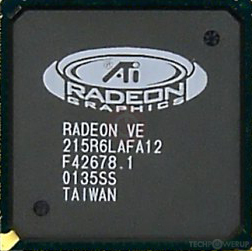
215R6WASA12

Radeon

Radeon VE

Die Shot
ATI's Rage 6 GPU uses the Rage 6 architecture and is made using a 180 nm production process at TSMC. With a die size of 115 mm² and a transistor count of 30 million it is a small chip. Rage 6 supports DirectX 7.0. Modern GPU compute technologies are not available. It features 2 pixel shaders and 1 vertex shaders, 6 texture mapping units and 2 ROPs. Due to the lack of unified shaders you will not be able to run recent games at all (which require unified shader/DX10+ support).
Graphics Processor
- Released
- Apr 1st, 2000
- GPU Name
- Rage 6
- Desktop Variant
- RV100
- Mobile Variant
- M6
- Codename
- Piglet
- Architecture
- Rage 6
- Foundry
- TSMC
- Process Size
- 180 nm
- Transistors
- 30 million
- Density
- 260.9K / mm²
- Die Size
- 115 mm²
Graphics Features
- DirectX
- 7.0
- OpenGL
- 1.3
- OpenCL
- N/A
- Vulkan
- N/A
- Pixel Shader
- 0.5
- Vertex Shader
- 1.1
- Compute
- GFX1
Render Config
- Pixel Shaders
- 2
- Vertex Shaders
- 1
- TMUs
- 6
- ROPs
- 2
- Max. TDP
- 23 W
All Rage 6 GPUs
ATI GPU Architecture History
Graphics cards using the ATI Rage 6 GPU
| Name | Chip | Memory | Shaders | TMUs | ROPs | GPU Clock | Memory Clock |
|---|---|---|---|---|---|---|---|
| 215R6WASA12 | 32 MB | 2 / 1 | 6 | 2 | 148 MHz | 148 MHz | |
| 215R6EBGA13 | 64 MB | 2 / 1 | 6 | 2 | 166 MHz | 166 MHz | |
| 215R6EBGA13 | 64 MB | 2 / 1 | 6 | 2 | 187 MHz | 180 MHz | |
| 215R6EBGA13 | 32 MB | 2 / 1 | 6 | 2 | 166 MHz | 166 MHz | |
| 215R6EBGA13 | 64 MB | 2 / 1 | 6 | 2 | 183 MHz | 183 MHz | |
| 215R6EBGA13 | 32 MB | 2 / 1 | 6 | 2 | 166 MHz | 166 MHz | |
| Radeon VE | 32 MB | 1 / 0 | 3 | 1 | 183 MHz | 183 MHz | |
| Radeon VE | 32 MB | 1 / 0 | 3 | 1 | 183 MHz | 183 MHz | |
| 215R6WASA12 | 32 MB | 2 / 1 | 6 | 2 | 148 MHz | 148 MHz | |
| 215R6EBGA13 | 32 MB | 2 / 1 | 6 | 2 | 166 MHz | 166 MHz |


Rage 6 GPU Notes
| Desktop Variant: RV100 Mobile Variant: M6 Codename: Piglet Graphics/Compute: GFX1 Charisma Engine Pixel Tapestry Video Immersion Fixed pipeline |
Jul 19th, 2024 08:23 EDT
change timezone
Latest GPU Drivers
New Forum Posts
- Include MSRP in the Specification table for every reviewed product (7)
- The TPU UK Clubhouse (25014)
- What's your latest tech purchase? (21087)
- Any other game like resident evil 1? (63)
- TPU's Nostalgic Hardware Club (18763)
- Upgrade from Acer XB271HUC IPS? (14)
- Can someone please give specs of Graphic variant 216-0867071 AMD? (2)
- Graphics card only runs with X1 instead X16 (31)
- What are you playing? (21119)
- DTS:X APO4 + DTS Interactive for Most Devices [USB Supported] (317)
Popular Reviews
- AMD Zen 5 Technical Deep Dive
- Noctua NH-D15 G2 Review - Big Performance, Bigger Price
- MCHOSE AX5 Pro Max Review
- Audeze MM-500 Open-Back Planar Magnetic Headphones Review
- Alphacool Core 1 LT CPU Water Block Review
- ID-Cooling FROZN A620 PRO SE Review - Better Value Than Thermalright
- Upcoming Hardware Launches 2024 (Updated May 2024)
- HIFIMAN Susvara Unveiled Planar Magnetic Headphones Review
- AMD Ryzen 7 7800X3D Review - The Best Gaming CPU
- The First Descendant Performance Benchmark Review - 30 GPUs Tested
Controversial News Posts
- Legendary Overclocker KINGPIN Leaves EVGA and Joins PNY to Develop Next-Generation GPUs for Extreme OC (195)
- NVIDIA GeForce RTX 50 Series "Blackwell" TDPs Leaked, All Powered by 16-Pin Connector (165)
- Noctua Announces $150 Flagship NH-D15 G2 CPU Coolers and NF-A14x25r G2 140mm Fans (164)
- Microsoft Closer to Removing Local Accounts from Windows 11, Removes Help Page on How to Switch to One (142)
- AMD is Becoming a Software Company. Here's the Plan (139)
- AMD to Revise Specs of Ryzen 7 9700X to Increase TDP to 120W, to Beat 7800X3D (112)
- Intel Planning P-core Only "Bartlett" LGA1700 Processor for 2025 (106)
- Intel "Arrow Lake-S" to See a Rearrangement of P-cores and E-cores Along the Ringbus (100)