Report an Error


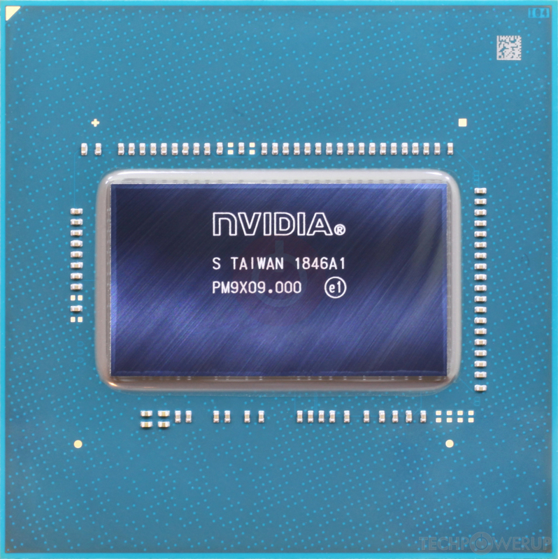
EVGA CMP 30HX
- Graphics Processor
- TU116
- Cores
- 1408
- TMUs
- 88
- ROPs
- 48
- Memory Size
- 6 GB
- Memory Type
- GDDR6
- Bus Width
- 192 bit
GPU
Graphics Processor
Graphics Card
Clock Speeds
- Base Clock
- 1530 MHz
- Boost Clock
- 1785 MHz
- Memory Clock
-
1750 MHz
14 Gbps effective
Memory
- Memory Size
- 6 GB
- Memory Type
- GDDR6
- Memory Bus
- 192 bit
- Bandwidth
- 336.0 GB/s
Render Config
- Shading Units
- 1408
- TMUs
- 88
- ROPs
- 48
- SM Count
- 22
- L1 Cache
- 64 KB (per SM)
- L2 Cache
- 1536 KB
Theoretical Performance
- Pixel Rate
- 85.68 GPixel/s
- Texture Rate
- 157.1 GTexel/s
- FP16 (half)
- 10.05 TFLOPS (2:1)
- FP32 (float)
- 5.027 TFLOPS
- FP64 (double)
- 157.1 GFLOPS (1:32)
Board Design
- Slot Width
- Dual-slot
- TDP
- 125 W
- Suggested PSU
- 300 W
- Outputs
- No outputs
- Power Connectors
- 1x 8-pin
- Board Number
- PG161 SKU 90
Graphics Features
- DirectX
- 12 (12_1)
- OpenGL
- 4.6
- OpenCL
- 3.0
- Vulkan
- 1.3
- CUDA
- 7.5
- Shader Model
- 6.8
TU116 GPU Notes
| NVENC: 7th Gen NVDEC: 4th Gen PureVideo HD: VP10 VDPAU: Feature Set J Latest Drivers: Windows 7 / 8 / 8.1 (x64): GeForce Release 474.89 Windows 10 / 11 (x64): GeForce Release: Latest |
Other retail boards based on this design (7)
| Name | GPU Clock | Boost Clock | Memory Clock | Other Changes |
|---|---|---|---|---|
| 1530 MHz | 1785 MHz | 1750 MHz | 242 mm/9.5 inches, Triple-slot | |
| 1530 MHz | 1785 MHz | 1750 MHz | ||
|
EVGA CMP 30HX
|
1530 MHz | 1785 MHz | 1750 MHz | |
| 1530 MHz | 1785 MHz | 1750 MHz | 225 mm/8.9 inches | |
| 1530 MHz | 1785 MHz | 1750 MHz | 244 mm/9.6 inches | |
| 1530 MHz | 1785 MHz | 1750 MHz | 207 mm/8.1 inches | |
| 1530 MHz | 1785 MHz | 1750 MHz |


Oct 18th, 2024 03:30 EDT
change timezone
Latest GPU Drivers
New Forum Posts
- Which 20 TB drive to get? (122)
- Help needed: can't get Realtek ALC1200 working on MSI B550M motherboard under Windows 7 (33)
- installing linux mint with some cinnamon on ssd (4)
- PSA: Do not buy from gigantti. (18)
- :O Limits of air cooling [Intel] (37)
- Ghetto Mods (4458)
- Post your Speedtest.net Speeds! (2308)
- DTS DCH Driver for Realtek HDA [DTS:X APO4 + DTS Interactive] (2002)
- Looking for a a new low power trio for my home studio (43)
- [Detailed + Need Help] Interesting Undervolting Lock(?) Situation on HP Victus 16 r1xxx (5)
Popular Reviews
- ASRock DeskMini X600 Barebones Mini-PC (Ryzen 8600G) Review
- Corsair 9000D RGB Airflow Review
- 64 Audio Solo Planar Magnetic IEMs Review
- Lian Li O11 Vision Compact Review
- Silent Hill 2 Remake Handheld Performance Review
- Logitech G Pro X Superlight 2 Review - Updated with 8000 Hz Tested
- Silent Hill 2 Remake Performance Benchmark Review - 35 GPUs Tested
- HAVN HS 420 VGPU Review
- Intel Core Ultra Arrow Lake Preview
- Montech King 65 Pro Review
Controversial News Posts
- NVIDIA GeForce RTX 5090 and RTX 5080 Specifications Surface, Showing Larger SKU Segmentation (183)
- AMD Ryzen 9 9950X3D and 9900X3D to Feature 3D V-cache on Both CCD Chiplets (127)
- Quick Denuvo DRM Cracks Cost Game Publishers 20% in Revenue, According to Study (125)
- MSI OCLab Reveals Ryzen 9000X3D 11-13% Faster Than 7000X3D, AMD Set to Dominate "Arrow Lake" in Gaming (123)
- AMD Rushing in Ryzen 7 9800X3D, Expect Product Launch Late-October (117)
- Single-Player Games Lose to PVP in Younger Audiences Despite Recent Hits (116)
- NVIDIA Tunes GeForce RTX 5080 GDDR7 Memory to 32 Gbps, RTX 5070 Launches at CES (112)
- Intel's Core Ultra 9 285K Performance Claims Leaked, Doesn't Beat i9-14900K at Gaming (111)