Report an Error


NVIDIA GeForce FX 5200
- Graphics Processor
- NV34
- Pixel Shaders
- 4
- Vertex Shaders
- 2
- TMUs
- 4
- ROPs
- 4
- Memory Size
- 128 MB
- Memory Type
- DDR
- Bus Width
- 128 bit

GPU
Recommended Gaming Resolutions:
- 640x480
- 1280x720
- 1366x768
The GeForce FX 5200 was a graphics card by NVIDIA, launched on March 6th, 2003. Built on the 150 nm process, and based on the NV34 graphics processor, in its NV34 5200 variant, the card supports DirectX 9.0a. Since GeForce FX 5200 does not support DirectX 11 or DirectX 12, it might not be able to run all the latest games. The NV34 graphics processor is an average sized chip with a die area of 124 mm² and 45 million transistors. It features 4 pixel shaders and 2 vertex shaders, 4 texture mapping units, and 4 ROPs. Due to the lack of unified shaders you will not be able to run recent games at all (which require unified shader/DX10+ support). NVIDIA has paired 128 MB DDR memory with the GeForce FX 5200, which are connected using a 128-bit memory interface. The GPU is operating at a frequency of 250 MHz, memory is running at 200 MHz.
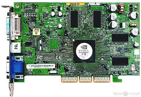
Being a single-slot card, the NVIDIA GeForce FX 5200 does not require any additional power connector, its power draw is not exactly known. Display outputs include: 1x DVI, 1x VGA, 1x S-Video. GeForce FX 5200 is connected to the rest of the system using an AGP 8x interface.
Being a single-slot card, the NVIDIA GeForce FX 5200 does not require any additional power connector, its power draw is not exactly known. Display outputs include: 1x DVI, 1x VGA, 1x S-Video. GeForce FX 5200 is connected to the rest of the system using an AGP 8x interface.
Graphics Processor
Graphics Card
- Release Date
- Mar 6th, 2003
- Generation
-
GeForce FX
(5200)
- Predecessor
- GeForce 4 Ti
- Successor
- GeForce 6 AGP
- Production
- End-of-life
- Bus Interface
- AGP 8x
Clock Speeds
- GPU Clock
- 250 MHz
- Memory Clock
-
200 MHz
400 Mbps effective
Memory
- Memory Size
- 128 MB
- Memory Type
- DDR
- Memory Bus
- 128 bit
- Bandwidth
- 6.400 GB/s
Render Config
- Pixel Shaders
- 4
- Vertex Shaders
- 2
- TMUs
- 4
- ROPs
- 4
Theoretical Performance
- Pixel Rate
- 1.000 GPixel/s
- Vertex Rate
- 125.0 MVertices/s
- Texture Rate
- 1.000 GTexel/s
Board Design
- Slot Width
- Single-slot
- TDP
- unknown
- Suggested PSU
- 200 W
- Outputs
- 1x DVI
1x VGA
1x S-Video
- Power Connectors
- None
Graphics Features
- DirectX
- 9.0a
- OpenGL
-
1.5 (full)
2.0 (partial)
- OpenCL
- N/A
- Vulkan
- N/A
- Pixel Shader
- 2.0a
- Vertex Shader
- 2.0a
NV34 GPU Notes
| Latest Drivers: Windows NT 4: ForceWare Release 77.56 ForceWare Release 77.72 Desktop Windows 95 / 98 / ME: ForceWare Release 81.98 Windows 2000: GeForce Release 93.71 / 93.81 Beta Quadro Release 169.96 Windows XP / Server 2003 x64: GeForce Release 175.19 Quadro Release 169.96 Windows Vista: ForceWare Release 96.85 |
Retail boards based on this design (5)
| Name | GPU Clock | Memory Clock | Other Changes |
|---|---|---|---|
| 250 MHz | 200 MHz | ||
| 250 MHz | 200 MHz | 2x VGA | |
| 250 MHz | 166 MHz | 1x VGA 1x S-Video, 64 bit | |
| 250 MHz | 200 MHz | 2x DVI 1x S-Video | |
| 250 MHz | 200 MHz | 1x DVI 1x VGA, 64 bit |


Nov 17th, 2024 18:21 EST
change timezone
Latest GPU Drivers
New Forum Posts
- No more driver beta testing programs (11)
- Crossfire R9 Fury not available (24)
- Dell Workstation Owners Club (3201)
- whats going on with core 2 quad and windows? (35)
- Anime Nation (12880)
- Help flashing Gigabyte AMD Radeon RX6600 eagle (20)
- Linpack Xtreme Released (483)
- Post your Cinebench R23 Score (3031)
- Your PC ATM (35022)
- RX 580 2048sp 8gb Problems (33)
Popular Reviews
- NVIDIA App v1.0 Review
- AMD Ryzen 7 9800X3D Review - The Best Gaming Processor
- Epomaker TH40 Wireless Mechanical Keyboard Review
- Redragon K1NG 8K Review
- Quick Look: MOONDROP Quark2 Type-C In-Ear Monitors
- Valkyrie VK02 Lite Review
- Beelink GTi12 Ultra Mini-PC + EX Dock (Intel Core i9-12900H) Review
- Upcoming Hardware Launches 2024 (Updated Nov 2024)
- NVIDIA GeForce RTX 4070 Super Founders Edition Review
- Quick Look: G.SKILL WigiDash PC Command Panel
Controversial News Posts
- AMD Falling Behind: Radeon dGPUs Absent from Steam's Top 20 (222)
- AMD Ryzen 7 9800X3D Stocks Vaporized in Retail, Being Scalped (151)
- AMD Introduces Next-Generation AMD Ryzen 7 9800X3D Processor, $479, Nov 7 (124)
- Apple and Samsung in the Fray to Acquire Intel: Rumor (123)
- AMD Ryzen 7 9800X3D Comes with 120W TDP, 5.20 GHz Boost, All Specs Leaked (120)
- Microsoft Offers $30 Windows 10 Security Extension for Home Users (118)
- AMD Ryzen 7 9800X3D Has the CCD on Top of the 3D V-cache Die, Not Under it (110)
- TechPowerUp is Hiring a Power Supply (PSU) Reviewer (106)