Report an Error


NVIDIA GeForce FX 5900
- Graphics Processor
- NV35
- Pixel Shaders
- 4
- Vertex Shaders
- 3
- TMUs
- 8
- ROPs
- 4
- Memory Size
- 128 MB
- Memory Type
- DDR
- Bus Width
- 256 bit

GPU
Recommended Gaming Resolutions:
- 640x480
- 1280x720
- 1366x768
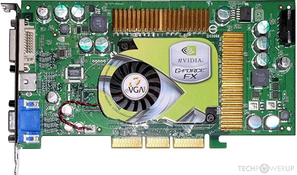
The GeForce FX 5900 was a high-end graphics card by NVIDIA, launched on May 12th, 2003. Built on the 130 nm process, and based on the NV35 graphics processor, in its FX 5900 variant, the card supports DirectX 9.0a. Since GeForce FX 5900 does not support DirectX 11 or DirectX 12, it might not be able to run all the latest games. The NV35 graphics processor is an average sized chip with a die area of 207 mm² and 135 million transistors. It features 4 pixel shaders and 3 vertex shaders, 8 texture mapping units, and 4 ROPs. Due to the lack of unified shaders you will not be able to run recent games at all (which require unified shader/DX10+ support). NVIDIA has paired 128 MB DDR memory with the GeForce FX 5900, which are connected using a 256-bit memory interface. The GPU is operating at a frequency of 400 MHz, memory is running at 425 MHz.
Being a single-slot card, the NVIDIA GeForce FX 5900 draws power from 1x Molex power connector, with power draw not exactly known. Display outputs include: 1x DVI, 1x VGA, 1x S-Video. GeForce FX 5900 is connected to the rest of the system using an AGP 8x interface. The card measures 218 mm in length, and features a single-slot cooling solution. Its price at launch was 399 US Dollars.
Being a single-slot card, the NVIDIA GeForce FX 5900 draws power from 1x Molex power connector, with power draw not exactly known. Display outputs include: 1x DVI, 1x VGA, 1x S-Video. GeForce FX 5900 is connected to the rest of the system using an AGP 8x interface. The card measures 218 mm in length, and features a single-slot cooling solution. Its price at launch was 399 US Dollars.
Graphics Processor
Graphics Card
- Release Date
- May 12th, 2003
- Generation
-
GeForce FX
(5900)
- Predecessor
- GeForce 4 Ti
- Successor
- GeForce 6 AGP
- Production
- End-of-life
- Launch Price
- 399 USD
- Bus Interface
- AGP 8x
- Reviews
- 11 in our database
Clock Speeds
- GPU Clock
- 400 MHz
- Memory Clock
-
425 MHz
850 Mbps effective
Memory
- Memory Size
- 128 MB
- Memory Type
- DDR
- Memory Bus
- 256 bit
- Bandwidth
- 27.20 GB/s
Render Config
- Pixel Shaders
- 4
- Vertex Shaders
- 3
- TMUs
- 8
- ROPs
- 4
Theoretical Performance
- Pixel Rate
- 1.600 GPixel/s
- Vertex Rate
- 300.0 MVertices/s
- Texture Rate
- 3.200 GTexel/s
Board Design
- Slot Width
- Single-slot
- Length
- 218 mm
8.6 inches
- TDP
- unknown
- Suggested PSU
- 200 W
- Outputs
- 1x DVI
1x VGA
1x S-Video
- Power Connectors
- 1x Molex
Graphics Features
- DirectX
- 9.0a
- OpenGL
-
1.5 (full)
2.0 (partial)
- OpenCL
- N/A
- Vulkan
- N/A
- Pixel Shader
- 2.0a
- Vertex Shader
- 2.0a
NV35 GPU Notes
| Latest Drivers: Windows NT 4: ForceWare Release 77.56 ForceWare Release 77.72 Desktop Windows 95 / 98 / ME: ForceWare Release 81.98 Windows 2000: GeForce Release 93.71 / 93.81 Beta Quadro Release 169.96 Windows XP / Server 2003 x64: GeForce Release 175.19 Quadro Release 169.96 Windows Vista: ForceWare Release 96.85 |
Retail boards based on this design (3)
| Name | GPU Clock | Memory Clock | Other Changes |
|---|---|---|---|
| 400 MHz | 425 MHz | ||
| 400 MHz | 425 MHz | ||
| 400 MHz | 425 MHz |


Oct 4th, 2024 22:14 EDT
change timezone
Latest GPU Drivers
New Forum Posts
- Silent Hill 2 Remake - Apparently really good (5)
- Solidigm NVMe Custom Modded Driver for All NVMe Brands SSDs & Any NVMe SSDs (48)
- New GameTech GPU benchmark. Share your results! (105)
- getting errors installing on 24h2 IoT Enterprise (15)
- 5500 XT or GTX 1650 for old PC? (73)
- TPU's Nostalgic Hardware Club (19168)
- Mobo Rear Panel USB 2.0 Ports In 2025 (61)
- BootLoop After Flashing My GPU !! (14)
- What are you playing? (21857)
- amdvbflash 4.104E for 64-bit linux with updated support for VBIOS Flash on Big Navi2x GPUs (7)
Popular Reviews
- ASUS ROG Crosshair X870E Hero Review
- Alphacool Apex Skeleton Review
- 2024 Shenzhen International Audio Show Report
- DDR5 Memory Performance Scaling with AMD Zen 5
- NZXT H7 Flow (2024) Review
- Lian Li Lancool 207 Review
- ASUS ROG Azoth Extreme Wireless Mechanical Keyboard Review
- ID-Cooling DX 360 MAX AIO Review
- Incott GHERO Pro Review
- Phison E31 PCIe 5.0 SSD Engineering Sample Preview - Impressive Efficiency
Controversial News Posts
- AMD Confirms Retreat from the Enthusiast GPU Segment, to Focus on Gaining Market-Share (266)
- Sony Reveals the PlayStation 5 Pro, Launches November 7th (216)
- NVIDIA GeForce RTX 5090 and RTX 5080 Specifications Surface, Showing Larger SKU Segmentation (180)
- AMD Ryzen 9 9950X3D and 9900X3D to Feature 3D V-cache on Both CCD Chiplets (126)
- Cyberpunk 2077 Update Adds AMD FSR 3 and Frame Generation for PC Players (122)
- AMD Rushing in Ryzen 7 9800X3D, Expect Product Launch Late-October (115)
- NVIDIA RTX 5090 "Blackwell" Could Feature Two 16-pin Power Connectors (109)
- Qualcomm Said to Have Approached Intel About Takeover Bid (102)