Report an Error

NVIDIA GeForce GT 640M
- Graphics Processor
- GK107
- Cores
- 384
- TMUs
- 32
- ROPs
- 16
- Memory Size
- 2 GB
- Memory Type
- DDR3
- Bus Width
- 128 bit
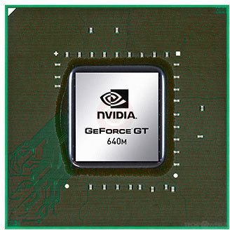

GPU
Recommended Gaming Resolutions:
- 1366x768
- 1600x900
- 1920x1080
The GeForce GT 640M was a mobile graphics chip by NVIDIA, launched on March 22nd, 2012. Built on the 28 nm process, and based on the GK107 graphics processor, in its N13P-GS variant, the chip supports DirectX 12. Even though it supports DirectX 12, the feature level is only 11_0, which can be problematic with newer DirectX 12 titles. The GK107 graphics processor is an average sized chip with a die area of 118 mm² and 1,270 million transistors. It features 384 shading units, 32 texture mapping units, and 16 ROPs. NVIDIA has paired 2,048 MB DDR3 memory with the GeForce GT 640M, which are connected using a 128-bit memory interface. The GPU is operating at a frequency of 624 MHz, which can be boosted up to 709 MHz, memory is running at 900 MHz.
Its power draw is rated at 32 W maximum. This device has no display connectivity, as it is not designed to have monitors connected to it. Rather it is intended for use in laptop/notebooks and will use the output of the host mobile device. GeForce GT 640M is connected to the rest of the system using a PCI-Express 3.0 x16 interface.
Its power draw is rated at 32 W maximum. This device has no display connectivity, as it is not designed to have monitors connected to it. Rather it is intended for use in laptop/notebooks and will use the output of the host mobile device. GeForce GT 640M is connected to the rest of the system using a PCI-Express 3.0 x16 interface.
Graphics Processor
Mobile Graphics
- Release Date
- Mar 22nd, 2012
- Generation
- GeForce 600M
- Predecessor
- GeForce 500M
- Successor
- GeForce 700M
- Production
- End-of-life
- Bus Interface
- PCIe 3.0 x16
- Reviews
- 2 in our database
Relative Performance
Based on TPU review data: "Performance Summary" at 1920x1080, 4K for 2080 Ti and faster.
Performance estimated based on architecture, shader count and clocks.
Clock Speeds
- Base Clock
- 624 MHz
- Boost Clock
- 709 MHz
- Memory Clock
-
900 MHz
1800 Mbps effective
Memory
- Memory Size
- 2 GB
- Memory Type
- DDR3
- Memory Bus
- 128 bit
- Bandwidth
- 28.80 GB/s
Render Config
- Shading Units
- 384
- TMUs
- 32
- ROPs
- 16
- SMX Count
- 2
- L1 Cache
- 16 KB (per SMX)
- L2 Cache
- 256 KB
Theoretical Performance
- Pixel Rate
- 5.672 GPixel/s
- Texture Rate
- 22.69 GTexel/s
- FP32 (float)
- 544.5 GFLOPS
- FP64 (double)
- 22.69 GFLOPS (1:24)
Board Design
- Slot Width
- IGP
- TDP
- 32 W
- Outputs
- Portable Device Dependent
- Power Connectors
- None
Graphics Features
- DirectX
- 12 (11_0)
- OpenGL
- 4.6
- OpenCL
- 3.0
- Vulkan
- 1.2.175
- CUDA
- 3.0
- Shader Model
- 6.5 (5.1)
Card Notes
| ???MHz core and 1000MHz memory clocks for the GDDR5 version, 625MHz/900MHz for the DDR3 version. |
GK107 GPU Notes
| NVENC: 1st Gen NVDEC: 1st Gen PureVideo HD: VP5 VDPAU: Feature Set D L1 Cache is configurable from 16 KB up to 48 KB per SMX Latest Drivers: Windows XP / Server 2003 x64: Quadro Release R319 U2 (321.01) Windows Vista: GeForce Release 365.19 Quadro Release R346 U7 (348.40) / R352 BETA (352.86) Windows 7 / 8 / 8.1 / 10 / 11 (x32 / x64): GeForce Release 391.35 / 475.06 Quadro Release R390 U9 (392.37) / R470 U16 (474.82) |
Nov 12th, 2024 17:34 EST
change timezone
Latest GPU Drivers
New Forum Posts
- Throttlestop overclocking Desktop PCs (1544)
- Different low reading (24)
- Only getting 2.5g Network one way (1)
- 9800x 3d vs 12900k - Battle of the Century (41)
- Asus GenZ.2 card thermal pad question (4)
- Dell Precision 5530 i7 8750H unable to undervolt using throttlestop? (1)
- New GameTech GPU benchmark. Share your results! (STEAM page live now) (140)
- sata ssd to usb-what have you found thats decently fast? (15)
- Inconsistent POSTing on PC ( already replaced multiple parts) (50)
- What's your latest tech purchase? (22244)
Popular Reviews
- AMD Ryzen 7 9800X3D Review - The Best Gaming Processor
- NVIDIA App v1.0 Review
- Team Group A440 Lite 2 TB Review
- FiiO Industrial Park/Factory Tour + Interview with Founder
- Upcoming Hardware Launches 2024 (Updated Nov 2024)
- MIRPH-1 Open-Back Dynamic Driver Headphones Review
- ID-Cooling FX360 INF AIO Review
- Dragon Age: The Veilguard Handheld Performance Review
- DDR5 Memory Performance Scaling with AMD Zen 5
- Intel Core Ultra 9 285K Review
Controversial News Posts
- AMD Falling Behind: Radeon dGPUs Absent from Steam's Top 20 (222)
- AMD Ryzen 7 9800X3D Stocks Vaporized in Retail, Being Scalped (140)
- Quick Denuvo DRM Cracks Cost Game Publishers 20% in Revenue, According to Study (136)
- AMD Introduces Next-Generation AMD Ryzen 7 9800X3D Processor, $479, Nov 7 (124)
- Apple and Samsung in the Fray to Acquire Intel: Rumor (123)
- AMD Ryzen 7 9800X3D Comes with 120W TDP, 5.20 GHz Boost, All Specs Leaked (120)
- Microsoft Offers $30 Windows 10 Security Extension for Home Users (118)
- AMD Ryzen 7 9800X3D Has the CCD on Top of the 3D V-cache Die, Not Under it (110)