Report an Error


HIS HD 2600 XT IceQ Turbo
- H260XTQT256DD-R
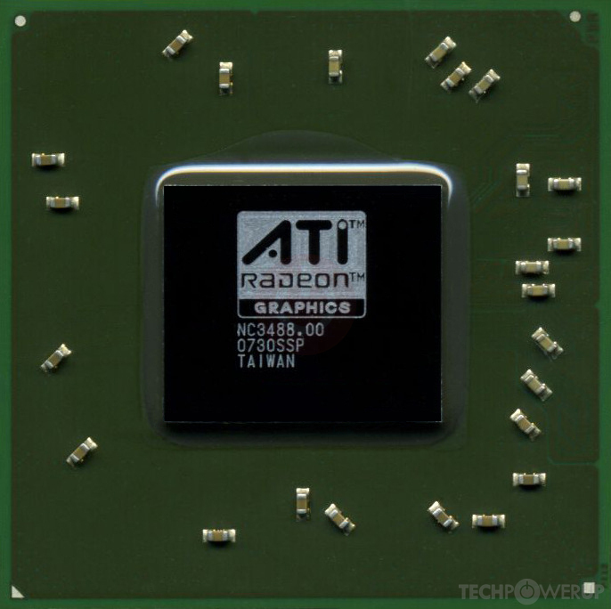
- Graphics Processor
- RV630
- Cores
- 120
- TMUs
- 8
- ROPs
- 4
- Memory Size
- 256 MB
- Memory Type
- GDDR3
- Bus Width
- 128 bit

GPU
Graphics Processor
Graphics Card
- Release Date
- Jun 28th, 2007
- Generation
-
Radeon R600
(HD 2600)
- Predecessor
- Radeon R500 PCIe
- Successor
- Radeon R700
- Production
- End-of-life
- Bus Interface
- PCIe 1.0 x16
Clock Speeds
- GPU Clock
800 MHz
830 MHz (+4%)
- Memory Clock
-
700 MHz
960 MHz (+37%)
1400 Mbps effective
1920 Mbps effective
Memory
- Memory Size
- 256 MB
- Memory Type
- GDDR3
- Memory Bus
- 128 bit
- Bandwidth
-
22.40 GB/s
30.72 GB/s
Render Config
- Shading Units
- 120
- TMUs
- 8
- ROPs
- 4
- Compute Units
- 3
- L2 Cache
- 64 KB
Theoretical Performance
- Pixel Rate
-
3.200 GPixel/s
3.320 GPixel/s
- Texture Rate
-
6.400 GTexel/s
6.640 GTexel/s
- FP32 (float)
-
192.0 GFLOPS
199.2 GFLOPS
Board Design
- Slot Width
Single-slot
Dual-slot
- TDP
- 45 W
- Suggested PSU
- 200 W
- Outputs
- 2x DVI
1x S-Video
- Power Connectors
- None
Graphics Features
- DirectX
- 10.0 (10_0)
- OpenGL
- 3.3
- OpenCL
- N/A
- Vulkan
- N/A
- Shader Model
- 4.0
Card Notes
| Variant Memory: 512 MB |
RV630 GPU Notes
| Mobile Variant: M76 Codename: Shaka Graphics/Compute: GFX3 Display Core Engine: 2.0 Unified Video Decoder: 1.0 RV630 Chip Numbers: RV630 XT (215CDABKA13FG) Latest Drivers: Windows XP / 8: Catalyst Software Suite 13.1 / 13.4 Beta Windows Vista / 7: Catalyst Software Suite 13.9 |
Other retail boards based on this design (2)
| Name | GPU Clock | Memory Clock | Other Changes |
|---|---|---|---|
|
HIS HD 2600 XT IceQ Turbo

|
830 MHz | 960 MHz | Dual-slot |
| 800 MHz | 700 MHz |

Jul 4th, 2024 10:58 EDT
change timezone
Latest GPU Drivers
New Forum Posts
- What are you playing? (20980)
- New GameTech GPU benchmark. Share your results! (16)
- Which ATX power supply (18)
- Assistance with identification, (4)
- Passmark Scores (38)
- What's your latest tech purchase? (20968)
- Windows 11 General Discussion (5214)
- Need help with i7-4700MQ (1)
- INNOCN 32M2V (0)
- The TPU UK Clubhouse (24938)
Popular Reviews
- Gigabyte GS34WQC Review - An Affordable Ultrawide
- AMD FidelityFX FSR 3.1 Review - Frame Generation for Everyone
- The First Descendant Performance Benchmark Review - 30 GPUs Tested
- Lian Li HydroShift LCD 360S AIO Review
- Upcoming Hardware Launches 2024 (Updated May 2024)
- Endgame Gear OP1 8K Review
- AMD Ryzen 7 7800X3D Review - The Best Gaming CPU
- XFX Radeon RX 7900 XTX Magnetic Air Review
- Thermalright Phantom Spirit 120 EVO Review
- Corsair MP600 Mini 2 TB Review - Great Storage for Steam Deck
Controversial News Posts
- Legendary Overclocker KINGPIN Leaves EVGA and Joins PNY to Develop Next-Generation GPUs for Extreme OC (195)
- Noctua Announces $150 Flagship NH-D15 G2 CPU Coolers and NF-A14x25r G2 140mm Fans (152)
- AMD Says Ryzen 9000 Series Won't Beat 7000X3D Series at Gaming (141)
- Possible Specs of NVIDIA GeForce "Blackwell" GPU Lineup Leaked (140)
- Microsoft Closer to Removing Local Accounts from Windows 11, Removes Help Page on How to Switch to One (128)
- First Reviews are Live and Snapdragon X Elite Doesn't Quite Deliver on Promised Performance (124)
- ASUS Enhances Customer Support Following Gamers Nexus Investigation (118)
- Nightmare Fuel for Intel: Arm CEO Predicts Arm will Take Over 50% Windows PC Market-share by 2029 (112)