Report an Error


HP HD 7650M 2 GB
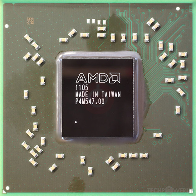
- Graphics Processor
- Thames
- Cores
- 480
- TMUs
- 24
- ROPs
- 16
- Memory Size
- 2 GB
- Memory Type
- HyperMemory
- Bus Width
- 128 bit

GPU
Graphics Processor
- GPU Name
- Thames
- GPU Variant
-
Thames M2 PRO
(216-0833002)
- Architecture
- TeraScale 2
- Foundry
- TSMC
- Process Size
- 40 nm
- Transistors
- 716 million
- Density
- 6.1M / mm²
- Die Size
- 118 mm²
- Chip Package
- FCBGA-631/962
Mobile Graphics
- Release Date
- Jan 7th, 2012
- Generation
-
London
(HD 7600M)
- Predecessor
- Vancouver
- Successor
- Solar System
- Production
- End-of-life
- Bus Interface
- PCIe 2.0 x16
Clock Speeds
- GPU Clock
- 500 MHz
- Memory Clock
-
800 MHz
900 MHz (+13%)
Memory
- Memory Size
-
1024 MB
2 GB
- Memory Type
DDR3
HyperMemory
- Memory Bus
- 128 bit
- Bandwidth
-
25.60 GB/s
14.40 GB/s
Render Config
- Shading Units
- 480
- TMUs
- 24
- ROPs
- 16
- Compute Units
- 6
- L1 Cache
- 8 KB (per CU)
- L2 Cache
- 256 KB
Theoretical Performance
- Pixel Rate
- 8.000 GPixel/s
- Texture Rate
- 12.00 GTexel/s
- FP32 (float)
- 480.0 GFLOPS
Board Design
- TDP
- 20 W
- Outputs
- Portable Device Dependent
Graphics Features
- DirectX
- 11.2 (11_0)
- OpenGL
- 4.4
- OpenCL
- 1.2
- Vulkan
- N/A
- Shader Model
- 5.0
Card Notes
| Memory Variant: 2048MB DDR3 Memory Variant: 1024MB GDDR3 Memory Variant: 2048MB GDDR3 |
Thames GPU Notes
| Generation: Northern Islands Desktop Variant: Turks Mobile Variant: Whistler Graphics/Compute: GFX4 Display Core Engine: 5.0 Unified Video Decoder: 3.1 |
Other retail boards based on this design (2)
| Name | GPU Clock | Memory Clock | Other Changes |
|---|---|---|---|
| 550 MHz | 800 MHz | ||
|
HP HD 7650M 2 GB

|
500 MHz | 900 MHz | 2 GB, HyperMemory |

Jul 16th, 2024 04:04 EDT
change timezone
Latest GPU Drivers
New Forum Posts
- External 8 TB SSDs before internal? (21)
- Alderon Games claims that substantial numbers of Intel 13th Gen and 14th Gen chips are defective (109)
- Windows 11 General Discussion (5228)
- What's your latest tech purchase? (21059)
- Which values are always 100% accurate? (2)
- TPU's Nostalgic Hardware Club (18751)
- UV and vramscaling 4070 super (6)
- Microsoft has locked me out of my own pc (99)
- AIR COOLING... what's the diference? (19)
- PC related hardware purchase that you regret very quickly after purchase. (167)
Popular Reviews
- AMD Zen 5 Technical Deep Dive
- HIFIMAN Susvara Unveiled Planar Magnetic Headphones Review
- Quick Look: Jelly Key Dragons of Eden Ethereal Runes Artisan Keycaps
- ID-Cooling FROZN A620 PRO SE Review - Better Value Than Thermalright
- HighPoint Rocket 1608A 8-Slot M.2 Gen 5 Review - 56 GB/s Transfer Rates
- The First Descendant Performance Benchmark Review - 30 GPUs Tested
- Upcoming Hardware Launches 2024 (Updated May 2024)
- AMD Ryzen 7 7800X3D Review - The Best Gaming CPU
- Corsair RS120 MAX 120 mm Fan Review
- XFX Radeon RX 7900 XTX Magnetic Air Review
Controversial News Posts
- Legendary Overclocker KINGPIN Leaves EVGA and Joins PNY to Develop Next-Generation GPUs for Extreme OC (195)
- Noctua Announces $150 Flagship NH-D15 G2 CPU Coolers and NF-A14x25r G2 140mm Fans (164)
- Microsoft Closer to Removing Local Accounts from Windows 11, Removes Help Page on How to Switch to One (142)
- AMD is Becoming a Software Company. Here's the Plan (139)
- NVIDIA GeForce RTX 50 Series "Blackwell" TDPs Leaked, All Powered by 16-Pin Connector (134)
- First Reviews are Live and Snapdragon X Elite Doesn't Quite Deliver on Promised Performance (124)
- AMD to Revise Specs of Ryzen 7 9700X to Increase TDP to 120W, to Beat 7800X3D (112)
- Intel "Arrow Lake-S" to See a Rearrangement of P-cores and E-cores Along the Ringbus (100)