Report an Error


MSI CMP 50HX MINER
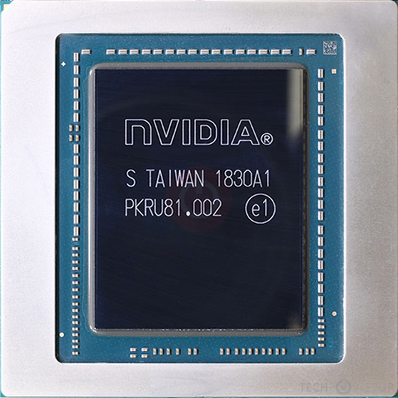
- Graphics Processor
- TU102
- Cores
- 3584
- TMUs
- 192
- ROPs
- 80
- Memory Size
- 10 GB
- Memory Type
- GDDR6
- Bus Width
- 320 bit

GPU

I/O

Top

Back
Graphics Processor
Graphics Card
Clock Speeds
- Base Clock
- 1350 MHz
- Boost Clock
- 1545 MHz
- Memory Clock
-
1750 MHz
14 Gbps effective
Memory
- Memory Size
- 10 GB
- Memory Type
- GDDR6
- Memory Bus
- 320 bit
- Bandwidth
- 560.0 GB/s
Render Config
- Shading Units
- 3584
- TMUs
- 192
- ROPs
- 80
- SM Count
- 56
- Tensor Cores
- 448
- RT Cores
- 56
- L1 Cache
- 64 KB (per SM)
- L2 Cache
- 5 MB
Theoretical Performance
- Pixel Rate
- 123.6 GPixel/s
- Texture Rate
- 296.6 GTexel/s
- FP16 (half)
- 22.15 TFLOPS (2:1)
- FP32 (float)
- 11.07 TFLOPS
- FP64 (double)
- 346.1 GFLOPS (1:32)
Board Design
- Slot Width
- Dual-slot
- Length
267 mm
268 mm
10.5 inches
10.6 inches
- Width
116 mm
114 mm
4.6 inches
4.5 inches
- Height
35 mm
36 mm
1.4 inches
- TDP
- 250 W
- Suggested PSU
- 600 W
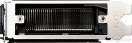
- Outputs
- No outputs
- Power Connectors
- 2x 8-pin
- Board Number
- PG150 SKU 100
Graphics Features
- DirectX
- 12 Ultimate (12_2)
- OpenGL
- 4.6
- OpenCL
- 3.0
- Vulkan
- 1.3
- CUDA
- 7.5
- Shader Model
- 6.7
TU102 GPU Notes
| Ray Tracing Cores: 1st Gen Tensor Cores: 2nd Gen NVENC: 7th Gen NVDEC: 4th Gen PureVideo HD: VP10 VDPAU: Feature Set J Latest Drivers: Windows 7 / 8 / 8.1 (x64): GeForce Release 474.89 Quadro Release R440 U3 (441.28) Data Center Release 426.32 Windows 10 / 11 (x64): GeForce Release: Latest Quadro Release: Latest Data Center Release: Latest |
Other retail boards based on this design (1)
| Name | GPU Clock | Boost Clock | Memory Clock | Other Changes |
|---|---|---|---|---|
|
MSI CMP 50HX MINER

|
1350 MHz | 1545 MHz | 1750 MHz | 268 mm/10.6 inches |
Jun 1st, 2024 13:05 EDT
change timezone
Latest GPU Drivers
New Forum Posts
- 3DMARK "LEGENDARY" (209)
- SPD Help (2)
- random shut down-PSU issue? (26)
- Would you pay more for hardware with AI capabilities? (86)
- 5700x at 100% on cyberpunk 2077 (0)
- Z890/X870 feature dreamlist (29)
- New Acer Helios 18 i9-14900hx constant throttle @ 94-100c (13)
- What are you playing? (20773)
- What is unverified VBIOS? (7)
- Best microATX case? (16)
Popular Reviews
- ID-Cooling FX360 PRO Review - Shots Fired @ Arctic
- SilverStone KL07E Review
- NuPhy Air96 V2 Low Profile Wireless Mechanical Keyboard Review
- Senua’s Saga: Hellblade II: DLSS vs. FSR vs. XeSS Comparison Review
- Upcoming Hardware Launches 2024 (Updated May 2024)
- Montech Titan Gold 1000 W Review
- Elysian Acoustic Labs Pilgrim In-Ear Monitors Review
- Waizowl OGM Cloud Review
- Ghost of Tsushima Performance Benchmark Review - 35 GPUs Tested
- Senua's Saga: Hellblade II Performance Benchmark Review
Controversial News Posts
- AMD to Redesign Ray Tracing Hardware on RDNA 4 (227)
- NVIDIA to Only Launch the Flagship GeForce RTX 5090 in 2024, Rest of the Series in 2025 (154)
- AMD Hits Highest-Ever x86 CPU Market Share in Q1 2024 Across Desktop and Server (140)
- AMD RDNA 5 a "Clean Sheet" Graphics Architecture, RDNA 4 Merely Corrects a Bug Over RDNA 3 (139)
- NVIDIA RTX 5090 "Blackwell" Founders Edition to Implement the "RTX 4090 Ti" Cinderblock Design (115)
- Core Configurations of Intel Core Ultra 200 "Arrow Lake-S" Desktop Processors Surface (101)
- Biden Administration to Revive Trump-Era Tariffs on China-made GPUs and Motherboards (95)
- NVIDIA Testing GeForce RTX 50 Series "Blackwell" GPU Designs Ranging from 250 W to 600 W (84)