Report an Error


NVIDIA TU102
TU102

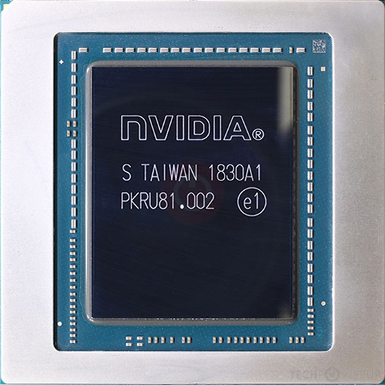
TU102-300A-K1-A1
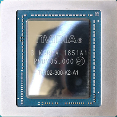
TU102-300-K2-A1

TU102-300-K3-A1

TU102-300-K5-A1

TU102-875-A1

TU102-890-KCD-A1

Die Shot

Block Diagram

SM Diagram
NVIDIA's TU102 GPU uses the Turing architecture and is made using a 12 nm production process at TSMC. With a die size of 754 mm² and a transistor count of 18,600 million it is a very big chip. TU102 supports DirectX 12 Ultimate (Feature Level 12_2). For GPU compute applications, OpenCL version 3.0 and CUDA 7.5 can be used. Additionally, the DirectX 12 Ultimate capability guarantees support for hardware-raytracing, variable-rate shading and more, in upcoming video games. It features 4608 shading units, 288 texture mapping units and 96 ROPs. Also included are 576 tensor cores which help improve the speed of machine learning applications. The GPU also contains 72 raytracing acceleration cores.
Further reading:
Turing Architecture Whitepaper 
Graphics Processor
- Released
- Aug 13th, 2018
- GPU Name
- TU102
- Codename
- NV162
- Architecture
- Turing
- Foundry
- TSMC
- Process Type
- 12FFN FinFET
- Process Size
- 12 nm
- Transistors
- 18,600 million
- Density
- 24.7M / mm²
- Die Size
- 754 mm²
Graphics Features
- DirectX
- 12 Ultimate (12_2)
- OpenGL
- 4.6
- OpenCL
- 3.0
- Vulkan
- 1.3
- CUDA
- 7.5
- Shader Model
- 6.7
- WDDM
- 3.1
- Tensor Cores
- 2nd Gen
- RT Cores
- 1st Gen
- NVENC
- 7th Gen
- NVDEC
- 4th Gen
- PureVideo HD
- VP10
- VDPAU
- Feature Set J
Render Config
- Shading Units
- 4608
- TMUs
- 288
- ROPs
- 96
- SM Count
- 72
- FP16 Units
- 9216
- FP64 Units
- 144
- INT32 Units
- 4608
- Tensor Cores
- 576
- RT Cores
- 72
- SFUs
- 1152
- TPCs
- 36
- GPCs
- 6
- Tex L1 Cache
- 32 KB per SM
- L1 Cache
- 64 KB per SM
- L2 Cache
- 6144 KB
- Max. TDP
- 280 W
All Turing GPUs
NVIDIA GPU Architecture History
- 2025 Blackwell 2.0
- 2024 Blackwell
- 2023 Hopper
- 2022-2024 Ada Lovelace
- 2020-2024 Ampere
- 2018-2022 Turing
- 2017-2020 Volta
- 2016-2021 Pascal
- 2014-2019 Maxwell 2.0
- 2014-2017 Maxwell
- 2013-2015 Kepler 2.0
- 2012-2018 Kepler
- 2010-2016 Fermi 2.0
- 2010-2013 VLIW Vec4
- 2010-2016 Fermi
- 2007-2013 Tesla 2.0
- 2006-2010 Tesla
- 2003-2013 Curie
- 2003-2005 Rankine
- 2001-2003 Kelvin
- 1999-2005 Celsius
- 1998-2000 Fahrenheit
Graphics cards using the NVIDIA TU102 GPU
| Name | Chip | Memory | Shaders | TMUs | ROPs | Base Clock | Boost Clock | Memory Clock |
|---|---|---|---|---|---|---|---|---|
| TU102-300A-K1-A1 | 11 GB | 4352 | 272 | 88 | 1350 MHz | 1545 MHz | 1750 MHz | |
| TU102-875-A1 | 48 GB | 4608 | 288 | 96 | 1395 MHz | 1770 MHz | 1750 MHz | |
| TU102-875-A1 | 24 GB | 4608 | 288 | 96 | 1440 MHz | 1770 MHz | 1750 MHz | |
| TU102-400-A1 | 24 GB | 4608 | 288 | 96 | 1350 MHz | 1770 MHz | 1750 MHz | |
| TU102-875-A1 | 24 GB | 4608 | 288 | 96 | 1305 MHz | 1560 MHz | 1750 MHz | |
| TU102-875-A1 | 48 GB | 4608 | 288 | 96 | 1230 MHz | 1620 MHz | 1625 MHz | |
| 24 GB | 4608 | 288 | 96 | 1275 MHz | 1455 MHz | 1750 MHz | ||
| TU102-875-A1 | 4 GB | 4608 | 288 | 96 | 1065 MHz | 1395 MHz | 1750 MHz | |
| TU102-875-A1 | 8 GB | 4608 | 288 | 96 | 1065 MHz | 1395 MHz | 1750 MHz | |
| TU102-875-A1 | 16 GB | 4608 | 288 | 96 | 1065 MHz | 1395 MHz | 1575 MHz | |
| TU102-100-A1 | 10 GB | 3584 | 192 | 80 | 1350 MHz | 1545 MHz | 1750 MHz | |
| TU102-875-A1 | 2 GB | 4608 | 288 | 96 | 1065 MHz | 1395 MHz | 1750 MHz | |
| TU102-350-A1 | 12 GB | 4608 | 288 | 96 | 1410 MHz | 1650 MHz | 2000 MHz | |
| 24 GB | 4608 | 288 | 96 | 1305 MHz | 1560 MHz | 1625 MHz | ||
| TU102-890-KCD-A1 | 16 GB | 3072 | 192 | 96 | 1065 MHz | 1395 MHz | 1575 MHz |


TU102 GPU Notes
| Ray Tracing Cores: 1st Gen Tensor Cores: 2nd Gen NVENC: 7th Gen NVDEC: 4th Gen PureVideo HD: VP10 VDPAU: Feature Set J Latest Drivers: Windows 7 / 8 / 8.1 (x64): GeForce Release 474.89 Quadro Release R440 U3 (441.28) Data Center Release 426.32 Windows 10 / 11 (x64): GeForce Release: Latest Quadro Release: Latest Data Center Release: Latest |
Jul 15th, 2024 20:18 EDT
change timezone
Latest GPU Drivers
New Forum Posts
- The Official Thermal Interface Material thread (1312)
- Microsoft has locked me out of my own pc (97)
- Alderon Games claims that substantial numbers of Intel 13th Gen and 14th Gen chips are defective (105)
- Have you got pie today? (16401)
- Milestones (13923)
- WCG Daily Numbers (12578)
- GPU missing a few capacitors/resistors near vram chips (3)
- TPU's Rosetta Milestones and Daily Pie Thread (1965)
- Folding Pie and Milestones!! (9091)
- Cooler Master X Silent Edge 1100W review (4)
Popular Reviews
- AMD Zen 5 Technical Deep Dive
- HIFIMAN Susvara Unveiled Planar Magnetic Headphones Review
- Quick Look: Jelly Key Dragons of Eden Ethereal Runes Artisan Keycaps
- ID-Cooling FROZN A620 PRO SE Review - Better Value Than Thermalright
- HighPoint Rocket 1608A 8-Slot M.2 Gen 5 Review - 56 GB/s Transfer Rates
- The First Descendant Performance Benchmark Review - 30 GPUs Tested
- Upcoming Hardware Launches 2024 (Updated May 2024)
- AMD Ryzen 7 7800X3D Review - The Best Gaming CPU
- Corsair RS120 MAX 120 mm Fan Review
- XFX Radeon RX 7900 XTX Magnetic Air Review
Controversial News Posts
- Legendary Overclocker KINGPIN Leaves EVGA and Joins PNY to Develop Next-Generation GPUs for Extreme OC (195)
- Noctua Announces $150 Flagship NH-D15 G2 CPU Coolers and NF-A14x25r G2 140mm Fans (164)
- Microsoft Closer to Removing Local Accounts from Windows 11, Removes Help Page on How to Switch to One (142)
- AMD is Becoming a Software Company. Here's the Plan (139)
- First Reviews are Live and Snapdragon X Elite Doesn't Quite Deliver on Promised Performance (124)
- NVIDIA GeForce RTX 50 Series "Blackwell" TDPs Leaked, All Powered by 16-Pin Connector (118)
- AMD to Revise Specs of Ryzen 7 9700X to Increase TDP to 120W, to Beat 7800X3D (112)
- Intel "Arrow Lake-S" to See a Rearrangement of P-cores and E-cores Along the Ringbus (100)