Report an Error


NVIDIA GT200B
GT200B

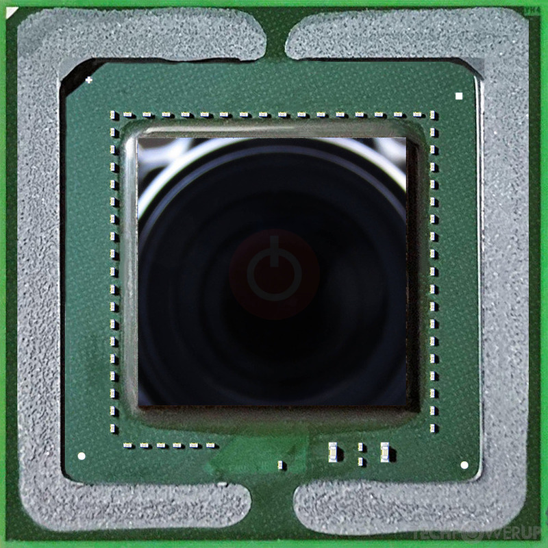
Heat Spreader

G200-105-B3

G200-350-B3

G200-400-B3
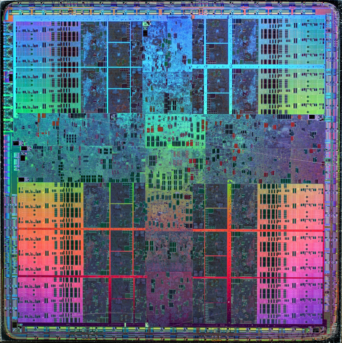
Fritzchens Fritz
Die Shot

Die TPC
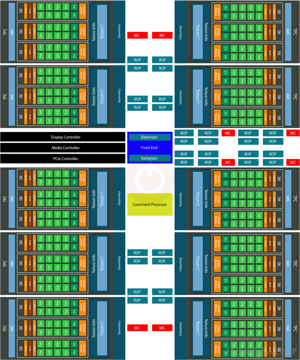
Block Diagram

TPC Diagram
NVIDIA's GT200B GPU uses the Tesla 2.0 architecture and is made using a 55 nm production process at TSMC. With a die size of 470 mm² and a transistor count of 1,400 million it is a very big chip. GT200B supports DirectX 11.1 (Feature Level 10_0). For GPU compute applications, OpenCL version 1.1 and CUDA 1.3 can be used. It features 240 shading units, 80 texture mapping units and 32 ROPs.
Graphics Processor
- Released
- Jun 1st, 2008
- GPU Name
- GT200B
- Codename
- NVA0
- Architecture
- Tesla 2.0
- Foundry
- TSMC
- Process Size
- 55 nm
- Transistors
- 1,400 million
- Density
- 3.0M / mm²
- Die Size
- 470 mm²
- Package
- BGA-1981
Graphics Features
- DirectX
- 11.1 (10_0)
- OpenGL
- 3.3
- OpenCL
- 1.1
- Vulkan
- N/A
- CUDA
- 1.3
- Shader Model
- 4.0
- WDDM
- 1.2
- PureVideo HD
- VP2
- VDPAU
- Feature Set A
Render Config
- Shading Units
- 240
- TMUs
- 80
- ROPs
- 32
- SM Count
- 30
- SFUs
- 60
- TPCs
- 10
- Tex L1 Cache
- 24 KB per TPC
- L2 Cache
- 256 KB
- Max. TDP
- 800 W
All Tesla 2.0 GPUs
NVIDIA GPU Architecture History
- 2025 Blackwell 2.0
- 2024 Blackwell
- 2023 Hopper
- 2022-2024 Ada Lovelace
- 2020-2024 Ampere
- 2018-2022 Turing
- 2017-2020 Volta
- 2016-2021 Pascal
- 2014-2019 Maxwell 2.0
- 2014-2017 Maxwell
- 2013-2015 Kepler 2.0
- 2012-2018 Kepler
- 2010-2016 Fermi 2.0
- 2010-2013 VLIW Vec4
- 2010-2016 Fermi
- 2007-2013 Tesla 2.0
- 2006-2010 Tesla
- 2003-2013 Curie
- 2003-2005 Rankine
- 2001-2003 Kelvin
- 1999-2005 Celsius
- 1998-2000 Fahrenheit
Graphics cards using the NVIDIA GT200B GPU
| Name | Chip | Memory | Shaders | TMUs | ROPs | GPU Clock | Memory Clock |
|---|---|---|---|---|---|---|---|
| G200-350-B3 | 1024 MB | 240 | 80 | 32 | 648 MHz | 1242 MHz | |
| G200-400-B3 | 896 MB | 240 | 80 | 28 | 576 MHz | 999 MHz | |
| G200-103-B2 | 896 MB | 216 | 72 | 28 | 576 MHz | 999 MHz | |
| G200-105-B3 | 896 MB | 240 | 80 | 28 | 633 MHz | 1134 MHz | |
| G200-350-B3 | 1024 MB | 240 | 80 | 32 | 648 MHz | 1242 MHz | |
| 4 GB | 240 | 80 | 32 | 648 MHz | 800 MHz | ||
| 4 GB | 240 | 80 | 32 | 648 MHz | 800 MHz | ||
| 4 GB | 240 | 80 | 32 | 610 MHz | 800 MHz | ||
| 1536 MB | 192 | 64 | 24 | 602 MHz | 800 MHz | ||
| G200-835-B2 | 1024 MB | 192 | 64 | 16 | 600 MHz | 800 MHz | |
| 1536 MB | 192 | 64 | 24 | 602 MHz | 800 MHz | ||
| 1536 MB | 192 | 64 | 24 | 602 MHz | 800 MHz | ||
| 1024 MB | 240 | 80 | 32 | 610 MHz | 800 MHz | ||
| 4 GB | 240 | 80 | 32 | 610 MHz | 800 MHz | ||
| 4 GB | 240 | 80 | 32 | 610 MHz | 800 MHz | ||
| 2 GB | 240 | 80 | 32 | 610 MHz | 800 MHz | ||
| G200-105-B3 | 896 MB | 240 | 80 | 28 | 633 MHz | 1134 MHz | |
| 4 GB | 240 | 80 | 32 | 610 MHz | 800 MHz | ||
| G200-103-B3 | 896 MB | 192 | 64 | 28 | 576 MHz | 999 MHz | |
| G200-350-B3 | 2 GB | 240 | 80 | 32 | 648 MHz | 1152 MHz | |
| G200-400-B3 | 896 MB | 240 | 80 | 28 | 576 MHz | 1008 MHz |


GT200B GPU Notes
| PureVideo HD: VP2 VDPAU: Feature Set A GT200B, commonly printed on the chip package as G200-xxx-Bx is an optical shrink of the G200 core to the newer 55 manufacturing process of TSMC. It helped shrink the core's energy and thermal footprints to a level that even facilitated building a dual-GPU accelerator Latest Drivers: Windows 2000: Quadro Release 261.19 Windows XP / Server 2003 x64: GeForce Release 185.81 (Notebooks) GeForce Release 340.52 Quadro Release R319 U2 (321.01) Tesla Release 258.96 Windows Vista: GeForce Release 307.83 (Notebooks) GeForce Release 342.01 Quadro Release R340 U15 (342.01) Tesla Release 258.96 Windows 7 / 8 / 8.1 / 10: GeForce Release 342.01 Quadro Release R340 U15 (342.01) Tesla Release 258.96 |
Nov 19th, 2024 08:21 EST
change timezone
Latest GPU Drivers
New Forum Posts
- New printer (39)
- RC Clubhouse! (217)
- 3D Printing ideas (7)
- PC freezes/ need to unplug HDMI cable! Mobo issue? what to do? (0)
- The TPU UK Clubhouse (25302)
- Technical Issues - TPU Main Site & Forum (2024) (376)
- What Was Your First... (Gaming Related Things) (38)
- Glass mousepad (5)
- What phone you use as your daily driver? And, a discussion of them. (1632)
- Steam Deck Owners Clubhouse (465)
Popular Reviews
- AMD Ryzen 7 9800X3D Review - The Best Gaming Processor
- Quick Look: MOONDROP Quark2 Type-C In-Ear Monitors
- Valkyrie VK02 Lite Review
- Beelink GTi12 Ultra Mini-PC + EX Dock (Intel Core i9-12900H) Review
- NVIDIA App v1.0 Review
- Quick Look: Shanling M1 Plus Portable Audio Player
- Epomaker TH40 Wireless Mechanical Keyboard Review
- Upcoming Hardware Launches 2024 (Updated Nov 2024)
- Redragon K1NG 8K Review
- Quick Look: G.SKILL WigiDash PC Command Panel
Controversial News Posts
- AMD Falling Behind: Radeon dGPUs Absent from Steam's Top 20 (222)
- AMD Ryzen 7 9800X3D Stocks Vaporized in Retail, Being Scalped (152)
- AMD Introduces Next-Generation AMD Ryzen 7 9800X3D Processor, $479, Nov 7 (124)
- Apple and Samsung in the Fray to Acquire Intel: Rumor (123)
- AMD Ryzen 7 9800X3D Comes with 120W TDP, 5.20 GHz Boost, All Specs Leaked (120)
- Microsoft Offers $30 Windows 10 Security Extension for Home Users (118)
- AMD Ryzen 7 9800X3D Has the CCD on Top of the 3D V-cache Die, Not Under it (110)
- TechPowerUp is Hiring a Power Supply (PSU) Reviewer (105)