Report an Error


AMD Radeon PRO V620
- Graphics Processor
- Navi 21
- Cores
- 4608
- TMUs
- 288
- ROPs
- 128
- Memory Size
- 32 GB
- Memory Type
- GDDR6
- Bus Width
- 256 bit

GPU

I/O

Back
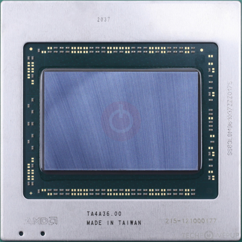
The Radeon PRO V620 is a professional graphics card by AMD, launched on November 4th, 2021. Built on the 7 nm process, and based on the Navi 21 graphics processor, in its Navi 21 XT variant, the card supports DirectX 12 Ultimate. The Navi 21 graphics processor is a large chip with a die area of 520 mm² and 26,800 million transistors. Unlike the fully unlocked Radeon RX 6900 XT, which uses the same GPU but has all 5120 shaders enabled, AMD has disabled some shading units on the Radeon PRO V620 to reach the product's target shader count. It features 4608 shading units, 288 texture mapping units, and 128 ROPs. The card also has 72 raytracing acceleration cores. AMD has paired 32 GB GDDR6 memory with the Radeon PRO V620, which are connected using a 256-bit memory interface. The GPU is operating at a frequency of 1825 MHz, which can be boosted up to 2200 MHz, memory is running at 2000 MHz (16 Gbps effective).
Being a dual-slot card, the AMD Radeon PRO V620 draws power from 2x 8-pin power connectors, with power draw rated at 300 W maximum. This device has no display connectivity, as it is not designed to have monitors connected to it. Radeon PRO V620 is connected to the rest of the system using a PCI-Express 4.0 x16 interface. The card's dimensions are 267 mm x 120 mm x 50 mm, and it features a dual-slot cooling solution.
Being a dual-slot card, the AMD Radeon PRO V620 draws power from 2x 8-pin power connectors, with power draw rated at 300 W maximum. This device has no display connectivity, as it is not designed to have monitors connected to it. Radeon PRO V620 is connected to the rest of the system using a PCI-Express 4.0 x16 interface. The card's dimensions are 267 mm x 120 mm x 50 mm, and it features a dual-slot cooling solution.
Graphics Processor
Graphics Card
- Release Date
- Nov 4th, 2021
- Generation
-
Radeon Pro Navi
(Navi II Series)
- Predecessor
- Radeon Pro Vega
- Production
- Active
- Bus Interface
- PCIe 4.0 x16
Relative Performance
Based on TPU review data: "Performance Summary" at 1920x1080, 4K for 2080 Ti and faster.
Performance estimated based on architecture, shader count and clocks.
Clock Speeds
- Base Clock
- 1825 MHz
- Boost Clock
- 2200 MHz
- Memory Clock
-
2000 MHz
16 Gbps effective
Memory
- Memory Size
- 32 GB
- Memory Type
- GDDR6
- Memory Bus
- 256 bit
- Bandwidth
- 512.0 GB/s
Render Config
- Shading Units
- 4608
- TMUs
- 288
- ROPs
- 128
- Compute Units
- 72
- RT Cores
- 72
- L0 Cache
- 32 KB per WGP
- L1 Cache
- 128 KB per Array
- L2 Cache
- 4 MB
- L3 Cache
- 128 MB
Theoretical Performance
- Pixel Rate
- 281.6 GPixel/s
- Texture Rate
- 633.6 GTexel/s
- FP16 (half)
- 40.55 TFLOPS (2:1)
- FP32 (float)
- 20.28 TFLOPS
- FP64 (double)
- 1,267 GFLOPS (1:16)
Board Design
- Slot Width
- Dual-slot
- Length
- 267 mm
10.5 inches
- Width
- 120 mm
4.7 inches
- Height
- 50 mm
2 inches
- TDP
- 300 W
- Suggested PSU
- 700 W
- Outputs
- No outputs
- Power Connectors
- 2x 8-pin
- Board Number
- 109-D60387-00_02
Graphics Features
- DirectX
- 12 Ultimate (12_2)
- OpenGL
- 4.6
- OpenCL
- 2.1
- Vulkan
- 1.3
- Shader Model
- 6.8
Navi 21 GPU Notes
| Generation: Navi II Codename: Sienna Cichlid / Gaming Ray Tracing Cores: 1st Gen Infinity Cache: 1st Gen Graphics/Compute: 10.3.0 Shader ISA: GFX10.3 (gfx1030) Display Core Next: 3.0.0 Video Core Next: 3.0.0 System DMA: 5.2.0 Platform Security Processor: 11.0.7 Per SIMD32: - 10 KB Scalar Register File Per CU: - 16 KB Vector Data Cache - 64 KB Local Data Share (GCN-Mode) Per WGP: - 16 KB Scalar Data Cache / K Cache - 32 KB Instruction Cache - 128 KB Local Data Share Latest Drivers: Windows 7: 64-bit: AMD Software: Adrenalin Edition 22.6.1 Windows 10 / 11: 64-bit: AMD Software: Adrenalin Edition: Latest 64-bit: AMD Software: PRO Edition 22.Q4 |
Sep 17th, 2024 01:04 EDT
change timezone
Latest GPU Drivers
New Forum Posts
- Bitcoin price prediction (40)
- mGPU in games such as Chernobylite on the 556 driver (1)
- Microsoft MUST provide Windows 10 updates for at least another 10 years (13)
- getting ready for dual 5090, Functional protype on dual 4090 (56)
- Samsung 870 EVO - Beware, certain batches prone to failure! (1210)
- Youtube, Discord, Visual Studio Code are flickering with black checkered squares/vertical lines. Partial solutions to this issue. (443)
- It checks out as authentic (23)
- Minimum or recommended voltages for VCCSA and VCCIO2 (Aux Mem) for 4 Hynix-D DDR4 RAM modules, in GEAR 1 (9)
- As we live the age of game remakes, which game you would like to see to have a remake? (272)
- Discord, Arduino, chromium crashing with fix. (3)
Popular Reviews
- Warhammer: Space Marine 2 Performance Benchmark Review - 35 GPUs Tested
- Warhammer 40000: Space Marine 2 Handheld Performance Review
- Titan Army P32A2S2 Review - Large Panel, Manageable Resolution
- Upcoming Hardware Launches 2024 (Updated Jul 2024)
- HYTE Y70 Review
- AMD Ryzen 9 9950X Review - The New Flagship
- MOONDROP COSMO Open-Back Planar Magnetic Headphones Review
- AMD Ryzen 7 7800X3D Review - The Best Gaming CPU
- ADATA Legend 970 Pro 2 TB Review
- AMD Radeon RX 7800 XT Review
Controversial News Posts
- AMD Confirms Retreat from the Enthusiast GPU Segment, to Focus on Gaining Market-Share (250)
- Sony Reveals the PlayStation 5 Pro, Launches November 7th (164)
- AnandTech Shuts Down, an Icon of Tech News and Reviews Rides into the Sunset (151)
- AMD Ryzen Branch Prediction Optimizations Now Available to Windows 11 23H2 (130)
- Cyberpunk 2077 Update Adds AMD FSR 3 and Frame Generation for PC Players (118)
- AMD Ryzen 5 7600X3D Launched in the US as a MicroCenter-exclusive for $300, Part of a Bundle (116)
- Report: Intel Could Spin Out Foundry Business or Cancel Some Expansion Plans to Control Losses (113)
- NVIDIA's RTX 5060 "Blackwell" Laptop GPU Comes with 8 GB of GDDR7 Memory Running at 28 Gbps, 25 W Lower TGP (108)