Report an Error


UNIKA PCX8628GTS
- PCX8628GTS
- Graphics Processor
- G84
- Cores
- 32
- TMUs
- 16
- ROPs
- 8
- Memory Size
- 256 MB
- Memory Type
- GDDR3
- Bus Width
- 128 bit

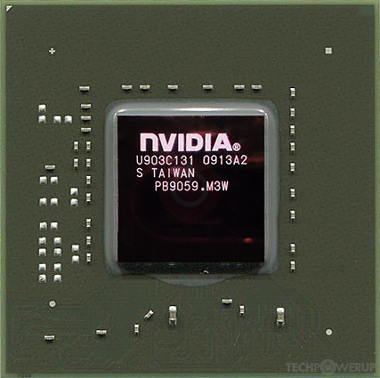
GPU
Graphics Processor
Graphics Card
- Release Date
- Apr 17th, 2007
- Generation
-
GeForce 8
(8600)
- Predecessor
- GeForce 7 PCIe
- Successor
- GeForce 9
- Production
- End-of-life
- Bus Interface
- PCIe 1.0 x16
Clock Speeds
- GPU Clock
- 675 MHz
- Shader Clock
- 1450 MHz
- Memory Clock
-
1000 MHz
2 Gbps effective
Memory
- Memory Size
- 256 MB
- Memory Type
- GDDR3
- Memory Bus
- 128 bit
- Bandwidth
- 32.00 GB/s
Render Config
- Shading Units
- 32
- TMUs
- 16
- ROPs
- 8
- SM Count
- 4
- L2 Cache
- 32 KB
Theoretical Performance
- Pixel Rate
- 5.400 GPixel/s
- Texture Rate
- 10.80 GTexel/s
- FP32 (float)
- 92.80 GFLOPS
Board Design
- Slot Width
- Single-slot
- TDP
- 60 W
- Suggested PSU
- 250 W
- Outputs
- 2x DVI
1x S-Video
- Power Connectors
- 1x 6-pin
- Board Number
- P401 SKU 0
Graphics Features
- DirectX
- 11.1 (10_0)
- OpenGL
- 3.3
- OpenCL
- 1.1
- Vulkan
- N/A
- CUDA
- 1.1
- Shader Model
- 4.0
Card Notes
| Memory Variant: 512 MB |
G84 GPU Notes
| PureVideo HD: VP2 VDPAU: Feature Set A Latest Drivers: Windows 2000: Quadro Release 261.19 Windows XP / Server 2003 x64: GeForce Release 340.52 Quadro Release R319 U2 (321.01) Tesla Release 258.96 Windows Vista / 7 / 8 / 8.1 / 10 32-bit: GeForce Release 342.01 Quadro Release R340 U15 (342.01) Tesla Release 258.96 |
Other retail boards based on this design (3)
| Name | GPU Clock | Memory Clock | Other Changes |
|---|---|---|---|
|
UNIKA PCX8628GTS

|
675 MHz | 1000 MHz | |
| 720 MHz | 1100 MHz | 196 mm/7.7 inches | |
| 720 MHz | 1100 MHz |


Jul 15th, 2024 21:53 EDT
change timezone
Latest GPU Drivers
New Forum Posts
- Excellent stability, low cost and low power consumption Bluetooth module TS-M1029D (0)
- How to fix performance issue (3)
- ARC "driver issues" turning out to be actually hardware deficiencies - Battlemage reveal (36)
- PC related hardware purchase that you regret very quickly after purchase. (161)
- Very poor performance with Intel core i5-11600KF with stock 4.9 GHz (61)
- The Official Thermal Interface Material thread (1316)
- WASD key lag in demanding games (Warzone, Dead Island 2, Fortnite) (4)
- Sexy Hardware Close-Up Pic Clubhouse. (10256)
- Alderon Games claims that substantial numbers of Intel 13th Gen and 14th Gen chips are defective (106)
- Microsoft has locked me out of my own pc (98)
Popular Reviews
- AMD Zen 5 Technical Deep Dive
- HIFIMAN Susvara Unveiled Planar Magnetic Headphones Review
- Quick Look: Jelly Key Dragons of Eden Ethereal Runes Artisan Keycaps
- ID-Cooling FROZN A620 PRO SE Review - Better Value Than Thermalright
- HighPoint Rocket 1608A 8-Slot M.2 Gen 5 Review - 56 GB/s Transfer Rates
- The First Descendant Performance Benchmark Review - 30 GPUs Tested
- Upcoming Hardware Launches 2024 (Updated May 2024)
- AMD Ryzen 7 7800X3D Review - The Best Gaming CPU
- Corsair RS120 MAX 120 mm Fan Review
- XFX Radeon RX 7900 XTX Magnetic Air Review
Controversial News Posts
- Legendary Overclocker KINGPIN Leaves EVGA and Joins PNY to Develop Next-Generation GPUs for Extreme OC (195)
- Noctua Announces $150 Flagship NH-D15 G2 CPU Coolers and NF-A14x25r G2 140mm Fans (164)
- Microsoft Closer to Removing Local Accounts from Windows 11, Removes Help Page on How to Switch to One (142)
- AMD is Becoming a Software Company. Here's the Plan (139)
- First Reviews are Live and Snapdragon X Elite Doesn't Quite Deliver on Promised Performance (124)
- NVIDIA GeForce RTX 50 Series "Blackwell" TDPs Leaked, All Powered by 16-Pin Connector (123)
- AMD to Revise Specs of Ryzen 7 9700X to Increase TDP to 120W, to Beat 7800X3D (112)
- Intel "Arrow Lake-S" to See a Rearrangement of P-cores and E-cores Along the Ringbus (100)