Report an Error
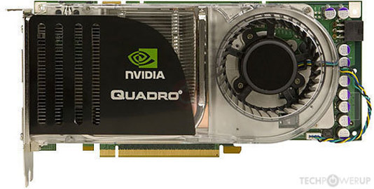


NVIDIA Quadro FX 4600
- Graphics Processor
- G80
- Cores
- 96
- TMUs
- 24
- ROPs
- 24
- Memory Size
- 768 MB
- Memory Type
- GDDR3
- Bus Width
- 384 bit


GPU
I/O
Recommended Gaming Resolutions:
- 1366x768
- 1600x900
- 1920x1080
The Quadro FX 4600 was an enthusiast-class professional graphics card by NVIDIA, launched on March 5th, 2007. Built on the 90 nm process, and based on the G80 graphics processor, in its G80-850-A2 variant, the card supports DirectX 11.1. Even though it supports DirectX 11, the feature level is only 10_0, which can be problematic with many DirectX 11 & DirectX 12 titles. The G80 graphics processor is a large chip with a die area of 484 mm² and 681 million transistors. Unlike the fully unlocked GeForce 8800 GTX, which uses the same GPU but has all 128 shaders enabled, NVIDIA has disabled some shading units on the Quadro FX 4600 to reach the product's target shader count. It features 96 shading units, 24 texture mapping units, and 24 ROPs. NVIDIA has paired 768 MB GDDR3 memory with the Quadro FX 4600, which are connected using a 384-bit memory interface. The GPU is operating at a frequency of 500 MHz, memory is running at 700 MHz.
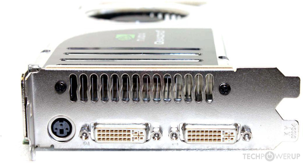
Being a dual-slot card, the NVIDIA Quadro FX 4600 draws power from 1x 6-pin power connector, with power draw rated at 134 W maximum. Display outputs include: 2x DVI, 1x S-Video. Quadro FX 4600 is connected to the rest of the system using a PCI-Express 1.0 x16 interface. The card measures 229 mm in length, 111 mm in width, and features a dual-slot cooling solution. Its price at launch was 1999 US Dollars.
Being a dual-slot card, the NVIDIA Quadro FX 4600 draws power from 1x 6-pin power connector, with power draw rated at 134 W maximum. Display outputs include: 2x DVI, 1x S-Video. Quadro FX 4600 is connected to the rest of the system using a PCI-Express 1.0 x16 interface. The card measures 229 mm in length, 111 mm in width, and features a dual-slot cooling solution. Its price at launch was 1999 US Dollars.
Graphics Processor
Graphics Card
- Release Date
- Mar 5th, 2007
- Generation
-
Quadro FX Tesla
(x600)
- Predecessor
- Quadro FX Rankine
- Successor
- Quadro Fermi
- Production
- End-of-life
- Launch Price
- 1,999 USD
- Bus Interface
- PCIe 1.0 x16
- Reviews
- 26 in our database
Relative Performance
Based on TPU review data: "Performance Summary" at 1920x1080, 4K for 2080 Ti and faster.
Performance estimated based on architecture, shader count and clocks.
Clock Speeds
- GPU Clock
- 500 MHz
- Shader Clock
- 1200 MHz
- Memory Clock
-
700 MHz
1400 Mbps effective
Memory
- Memory Size
- 768 MB
- Memory Type
- GDDR3
- Memory Bus
- 384 bit
- Bandwidth
- 67.20 GB/s
Render Config
- Shading Units
- 96
- TMUs
- 24
- ROPs
- 24
- SM Count
- 12
- L2 Cache
- 96 KB
Theoretical Performance
- Pixel Rate
- 12.00 GPixel/s
- Texture Rate
- 24.00 GTexel/s
- FP32 (float)
- 230.4 GFLOPS
Board Design
- Slot Width
- Dual-slot
- Length
- 229 mm
9 inches
- Width
- 111 mm
4.4 inches
- TDP
- 134 W
- Suggested PSU
- 300 W
- Outputs
- 2x DVI
1x S-Video
- Power Connectors
- 1x 6-pin
- Board Number
- Q356 SKU 0
Graphics Features
- DirectX
- 11.1 (10_0)
- OpenGL
- 3.3
- OpenCL
- 1.1 (1.0)
- Vulkan
- N/A
- CUDA
- 1.0
- Shader Model
- 4.0
G80 GPU Notes
| Each Streaming Multiprocessor(SM) in the chip architecture contains 8 SPs and 2 SFUs. Each SP can fulfill up to two single precision operations MAD per clock. Each SFU can fulfill up to four operations SF per clock (these units can also handle single-precision floating-point multiplications per clock). The approximate ratio of operations MAD to operations SF is equal 2:1. The theoretical SP + SFU performance in single-precision floating point operations [FLOPSsp + sfu, GFLOPS] of the graphics card with shader count [n] and shader frequency [f, GHz], is estimated by the following formula: FLOPSsp+sfu; f × n × 3. Alternative formula: FLOPSsp+sfu; f × m × ( 8 SPs * 2 (MAD) + 4 * 2 SFUs ). [m] - SM count. SP - Shader Processor (Unified Shader, CUDA Core) SFU - Special Function Unit SM - Streaming Multiprocessor MAD - ADD+MUL Latest Drivers: Windows 2000: Quadro Release 261.19 Windows XP / Server 2003 x64: GeForce Release 340.52 Quadro Release R319 U2 (321.01) Tesla Release 258.96 Windows Vista / 7 / 8 / 8.1 / 10 32-bit: GeForce Release 342.01 Quadro Release R340 U15 (342.01) Tesla Release 258.96 |
Apr 15th, 2025 09:02 EDT
change timezone
Latest GPU Drivers
New Forum Posts
- Thermaltake riing plus 12 rgb and other rgb fans. (7)
- Overclocking Micron F-die RAM (6)
- RX 9000 series GPU Owners Club (320)
- SK hynix A-Die (Overclocking thread) only for RYZEN AM5 users (36)
- Lian Li O11 Dynamic XL ROG. (18)
- DTS DCH Driver for Realtek HDA [DTS:X APO4 + DTS Interactive] (2136)
- Whats your favourite Linux Distro? (226)
- Need some help with vbios flashing (4)
- Asus ZenWifi BE14000 3pk or Orbi 770 3pk (2)
- The VHS to PC struggle (26)
Popular Reviews
- G.SKILL Trident Z5 NEO RGB DDR5-6000 32 GB CL26 Review - AMD EXPO
- ASUS GeForce RTX 5080 TUF OC Review
- Thermaltake TR100 Review
- The Last Of Us Part 2 Performance Benchmark Review - 30 GPUs Compared
- TerraMaster F8 SSD Plus Review - Compact and quiet
- DAREU A950 Wing Review
- Sapphire Radeon RX 9070 XT Pulse Review
- Zotac GeForce RTX 5070 Ti Amp Extreme Review
- Sapphire Radeon RX 9070 XT Nitro+ Review - Beating NVIDIA
- Upcoming Hardware Launches 2025 (Updated Apr 2025)
Controversial News Posts
- NVIDIA GeForce RTX 5060 Ti 16 GB SKU Likely Launching at $499, According to Supply Chain Leak (182)
- NVIDIA Sends MSRP Numbers to Partners: GeForce RTX 5060 Ti 8 GB at $379, RTX 5060 Ti 16 GB at $429 (124)
- Nintendo Confirms That Switch 2 Joy-Cons Will Not Utilize Hall Effect Stick Technology (105)
- Over 200,000 Sold Radeon RX 9070 and RX 9070 XT GPUs? AMD Says No Number was Given (100)
- Nintendo Switch 2 Launches June 5 at $449.99 with New Hardware and Games (99)
- Sony Increases the PS5 Pricing in EMEA and ANZ by Around 25 Percent (85)
- NVIDIA PhysX and Flow Made Fully Open-Source (77)
- NVIDIA Pushes GeForce RTX 5060 Ti Launch to Mid-April, RTX 5060 to May (77)